Overclocking the Sapphire NITRO RX Vega 64
To perform the overclocking on this graphics card, I used the Global WattMan utility built into the Radeon Settings app. I also use TechPowerUp’s GPU-Z utility, and its logging function to track GPU-only power draw, GPU frequency, and temperatures.
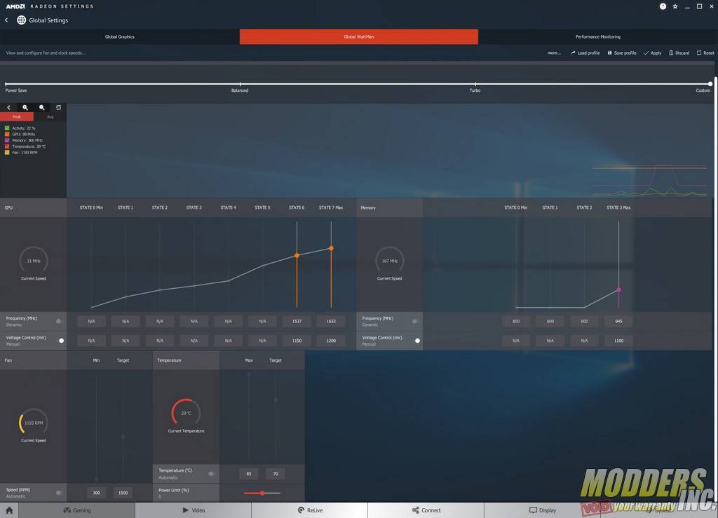
With the Boost BIOS active on the graphics card, the Dynamic Frequency for State 7 (maximum) was 1,632MHz at 1,200mV. The HBM’s default settings were 945MHz at 1,100mV for State 3 (maximum). The temperature target was set to 70°C, and the default power limit was 0%.
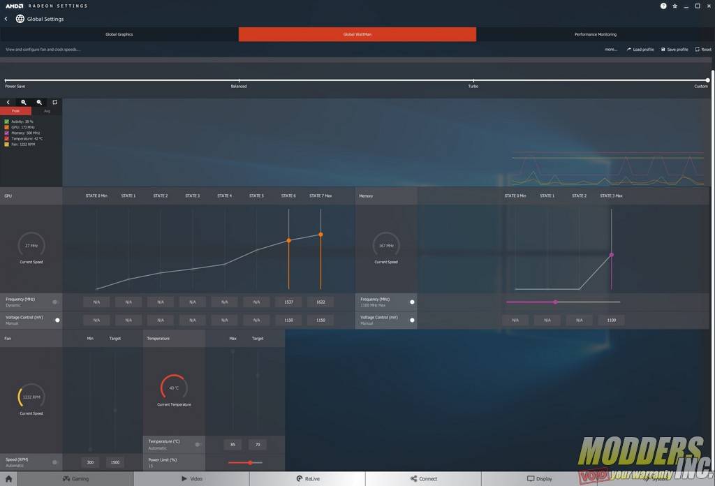
My goal was to limit power consumption to 300-watts (the air-cooled reference design has a Typical Board Power rating of 295-watts), while also getting a decent improvement in benchmark scores. I used 3DMark Fire Strike to validate my overclock. I raised the Power Limit percentage to 50% and moved the GPU and HBM frequency sliders around, but was consistently drawing more power than I wanted with too little performance benefit. When I started backing off the power limits, setting it to a more modest 15%, I was able to get better scores after actually lowering the GPU voltage by 50mV, cutting back the State 7 clock to 1,622MHz, raising the HBM clock to 1,100MHz, and leaving the memory voltage control at the default. Although lowering the core frequency isn’t my usual overclocking technique, GPU-Z never showed the frequency above 1,615MHz anyway. Indeed, AMD’s RX Vega appears to perform rather well when undervolted.
In 3DMark Fire Strike, the overall and graphics scores improved under my tweaked settings by 545 and 1,133 points, respectively.





I Want to know the name of this part in pcb marked in the picture in link.
>> https://drive.google.com/file/d/1bbyGGddJD1YUuHUoGRL_gzSIEsZxyM_O/view?usp=sharing