PowerColor R9 285 2GB Turbo Duo Review: It Takes Two to Tonga
A Closer Look at the PowerColor Radeon R9 285 TurboDuo Video Card
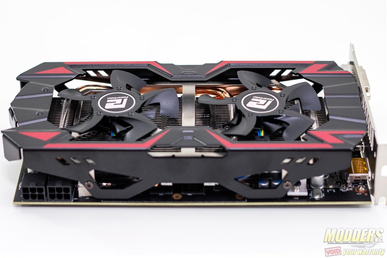
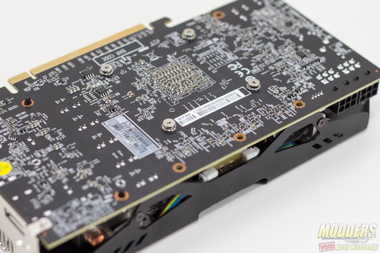
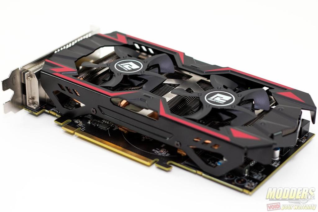
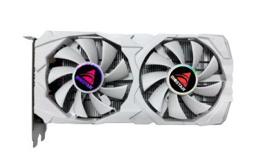
The PowerColor R9 285 TurboDuo OC is a dual-slot 38mm tall video card measuring 218mm in total length and 111.15mm wide. The dual-fan shroud extends the length longer than the PCB by 11mm (PCB length is 207mm). The back PCB is exposed with no backplate present or any spine reinforcement typically found on higher-end cards but there are unused mounting holes on the PCB for any creative modder to mount their home-made spine or backplate to. The entire card weighs only 327 grams.
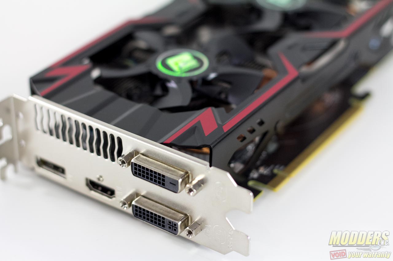
Rear connectors include all the standards for an R9 285: A DisplayPort connector, an HDMI 1.4a compatible connector, a dual-link DVI-I and a dual-link DVI-D. The HDMI and DisplayPort supports 3840×2160 4K displays simultaneously while the dual-link DVI ports max out at 2560×1600. Any three of the four display outputs can be run simultaneously for an AMD EyeFinity setup.
There are a pair of 6-pin power connectors on the side edge, each feeding 75W of additional power on top of the 75W from the PCI-E for a total of 225W for the video card.
There are no CrossFire connectors on the bottom side edge because unlike previous generation Radeon video cards, the R9 285 GPU has an XDMA (Xfire Direct Memory Access) engine in its display controller block that negotiates between the two cards through PCI-E 3.0 bus.
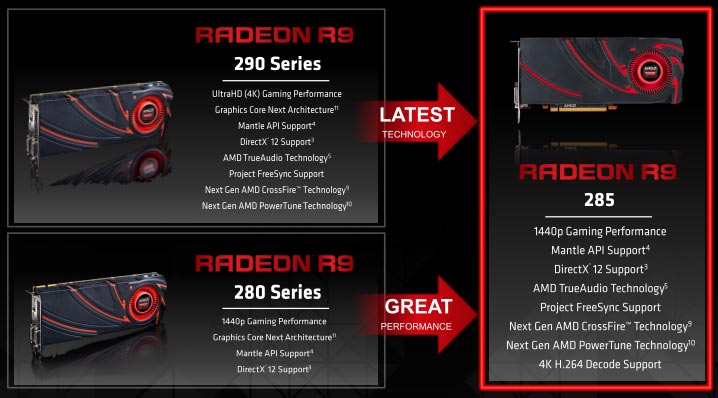
Before delving into the specifics of the PowerColor R9 285 video card components, understanding where the R9 285 (codename: “Tonga”) GPU fits in the big picture is essential. Slotted in between the R9 280 “Tahiti” and R9 290 “Hawaii” GPUs, the Tonga GPU sports the latest in AMD Radeon technology which explain why some of the specs seem redundant and even seem like a step back looking at the feature comparison table below:
| AMD Radeon R9 280 | AMD Radeon R9 280X | AMD Radeon R9 285 | |
| GPU Core | Tahiti Pro | Tahiti XT | Tonga |
| GPU Process | 28nm | 28nm | 28nm |
| GPU Cores | 1792 | 2048 | 1792 |
| Core Clock | 933 MHz | 1000 MHz | 918 MHz |
| VRAM | 3 GB GDDR5 | 3 GB GDDR5 | 2 GB GDDR5 |
| Memory Clock | 1250 MHz | 1500 MHz | 1375 MHz |
| Memory Bus | 384-bit | 384-bit | 256-bit |
| Memory Bandwidth | 224.4 GB/s | 288.0 GB/s | 176.2 GB/s |
| TMUs / ROPs | 116 / 32 | 128 / 32 | 112 / 32 |
The R9 285 Tonga is made by Taiwan Semiconductor MC with the same 28nm fabrication process node as R9 280 and R9 290 but the die size is slightly smaller at only 359mm2 compared to 365mm2 in the Tahiti and 438mm2 with Hawaii. Despite this, the Tonga is more complex than Tahiti with approximately 690 million more transistors. The R9 280 Tahiti is being phased out and replaced by the R9 285 that is why it is roughly in the same GPU class.
The Tonga GPU, being the most recent addition, is a lot more refined in terms of features and has new tricks up its sleeve that give it an advantage over the previously released Radeon GPUs. This is why the R9 285 only has a 256-bit memory interface compared to Tahiti’s 384-bit and sports a 2GB frame buffer compared to 3GB; AMD has introduced a new delta-based color compression engine that compensates for the narrower memory interface. These efficiencies are similar to techniques used by current mobile GPUs and NVIDIA’s latest efforts with their Maxwell GPUs. The R9 285 also inherits the Hawaii’s geometry front-end, theoretically double the throughput of Tahiti. Aside from the geometric and compression improvements, the R9 285 GPU also finally brings big updates to video decode performance with the Unified Video Decoder now fully supporting 4K H.264 up to level 5.2.
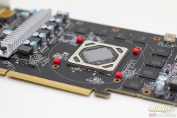
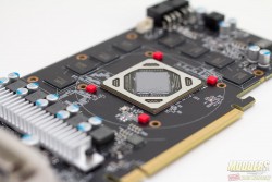
The TurboDuo cooling system has a copper plate on top of the Tonga GPU with medium-consistency gray Thermal Interface material in between them. The four red small foam pads around the GPU are for additional support around the sides since the copper plate is much larger than the GPU. The GPU MOSFET VRMs have their own little aluminum heatsink as well, attached via pushpins and moist gummy thermal tape between them. There are no pads directly on the memory but the TurboDuo fans blow down through and provide active cooling as well.
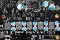
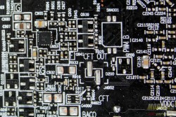
GPU VRM consists of an ON Semiconductor NCP81022, a 4+1 SVI2 controller utilizing one On-semi NTMFS4983NF and one NTMFS4C13N Power MOSFETs per phase, driven by ON-Semi NCP5901B drivers at the back. All capacitors are solid caps with 270uF 16V rating for the input power (with 0.47uH inductors) and 820uF 2.5V (with 0.15nH chokes) for the output filter. PLL power has an Anpec APW8713 with a 1.0uH inductor.
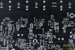
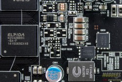
Memory VRM is a single-phase ON-Semi NCP5230 on the back PCB for the NTMFS4C05N and NTMFS4C13N Power MOSFET on the other side (NCP5230 has integrated driver). Output uses a Coiltronic 0.23uH Flat-PAC inductor with a pair of 820uF 2.5V capacitors. This VRM feeds the eight Elpida W2032BBBG-6A-F GDDR5 memory chips (2GB GDDR5 total) surrounding the GPU. The “2032” in the marking refers to density and organization while the “6A” refers to the 6.0 Gb/s speed rating.
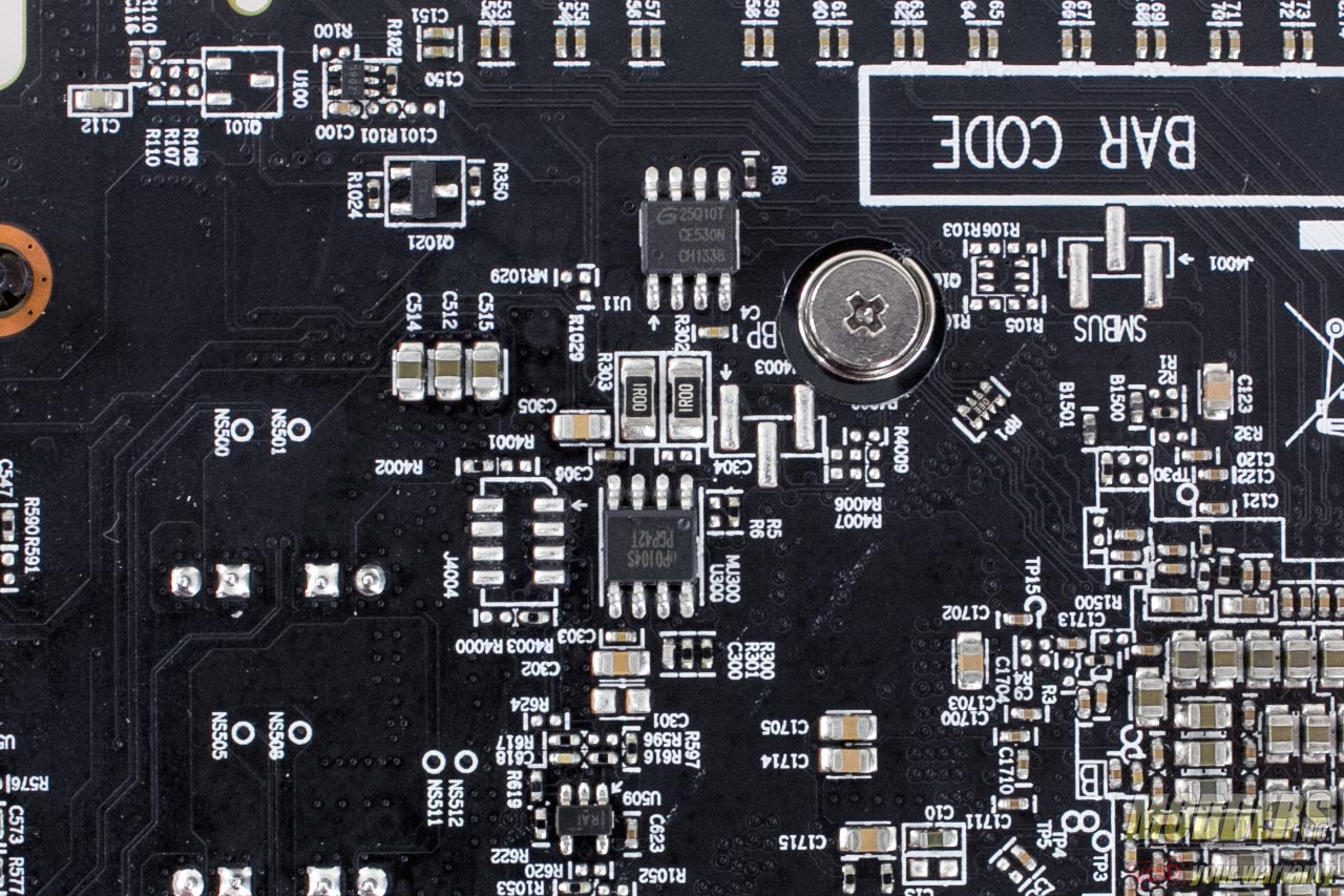
Of the two SO8 packages in the back of the PCB around the GPU area, the one closest to the PCI-E connector is the BIOS IC. This is a Gigadevice G25Q10 1Mbit 128KB serial flash chip.
