MSI 970 GAMING Motherboard Review
A Closer Look at the MSI 970 GAMING Motherboard
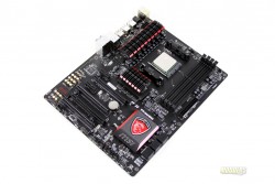
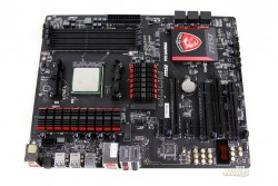
The MSI 970 GAMING motherboard uses a standard ATX form factor on a matte black 4-layer PCB. As with other MSI GAMING motherboards, the design follows a red and black theme with white lettering. This would look great with either a black or white case. Looking closely at the board I couldn’t find a physical power, reset buttons or a button for overclocking. There is no BIOS post codes on this board either. However, you can find them in the lower right corner of your screen when the system boots.
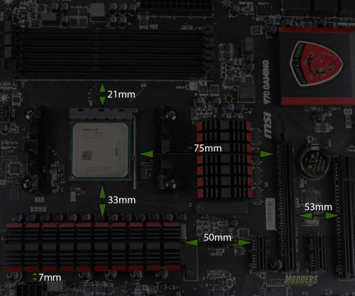 |
The CPU socket has a good clearance so you can use a large air cooler or even a liquid cooler.
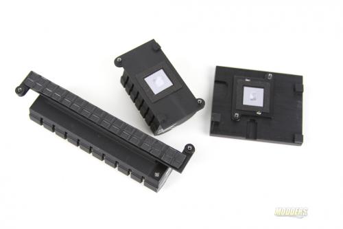 |
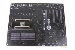
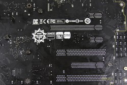
The MSI 970 GAMING has passive cooling on MOSFET, AMD970 and AMD SB950 bridges. These heat sinks are held in place by spring loaded screws from the back of the board, but they are not connected via heat pipes. Thermal padding was also found on North and South bridges along with MOSFET. Keeping both bridges cooled is important; however keeping MOSFETs cooled is a priority. If you plan to overclock keep in mind that excellent MOSFET cooling is essential to optimal power delivery for FX processor overclocking.
The MSI 970 Gaming uses a UPI uP1601p PWM controller capable of up to 4+2 phases but since the CPU VRM has 6+2 phases, only three phases are used on the first rail for the CPU and doublers are used to get 6-phases. The other two phases are used for the CPUNB. Each phase has a pair of NIKO Semiconductor PK632BA and PK616BA MOSFETs driven by a UPI uP1951 driver. Output filtering consists of eight 0.47uH “super-ferrite” chokes and 13x 560uF capacitors.
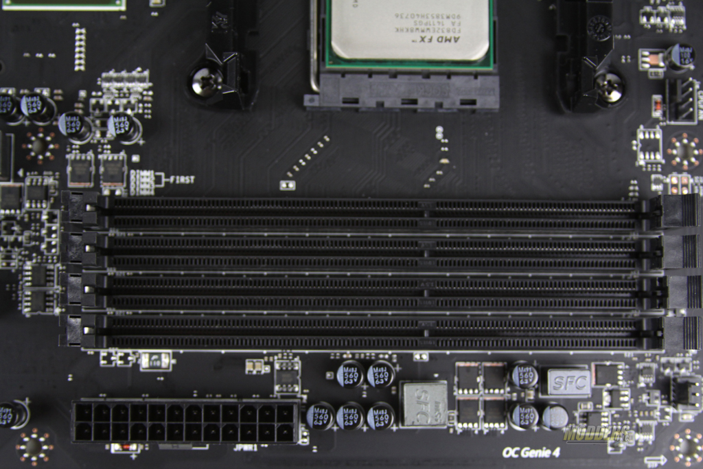
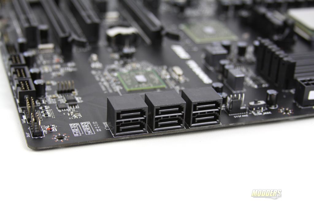
There are four DIMM slots supporting up to 32GB of DDR3 at 2133MHz (8GB per DIMM). The 24-pin CPU connector is also at the right side edge. Continuing on below that are the six SATA3 6Gbps connectors, natively provided by the AMD SB950 chipset. There are no additional storage options for SATA Express or M.2 NGFF (Next Generation Form Factor) connections. Between the 24-pin power connector and the SATA ports is a Slow-mode toggle switch for LN2 overclockers.
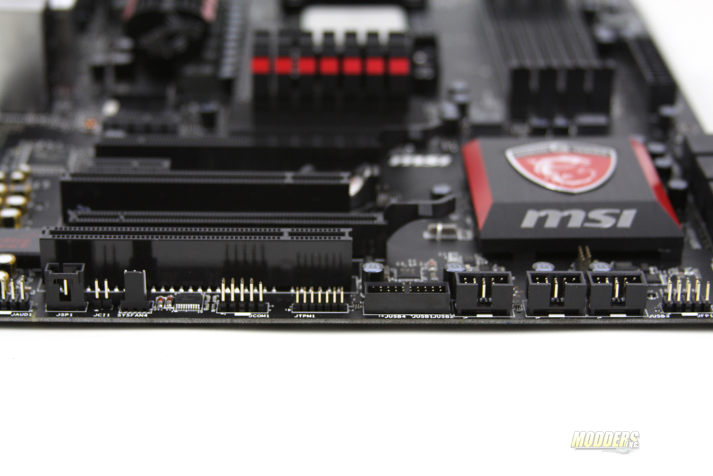
Along the bottom edge starting from the right side, there are a pair of front panel connector ports, three 9-pin USB 2.0 header, a 19-pin USB 3.0 header, a Trusted Platform Module header and a COM port. The USB 2.0 ports are natively provided by the SB950 chipset while the USB 3.0 port
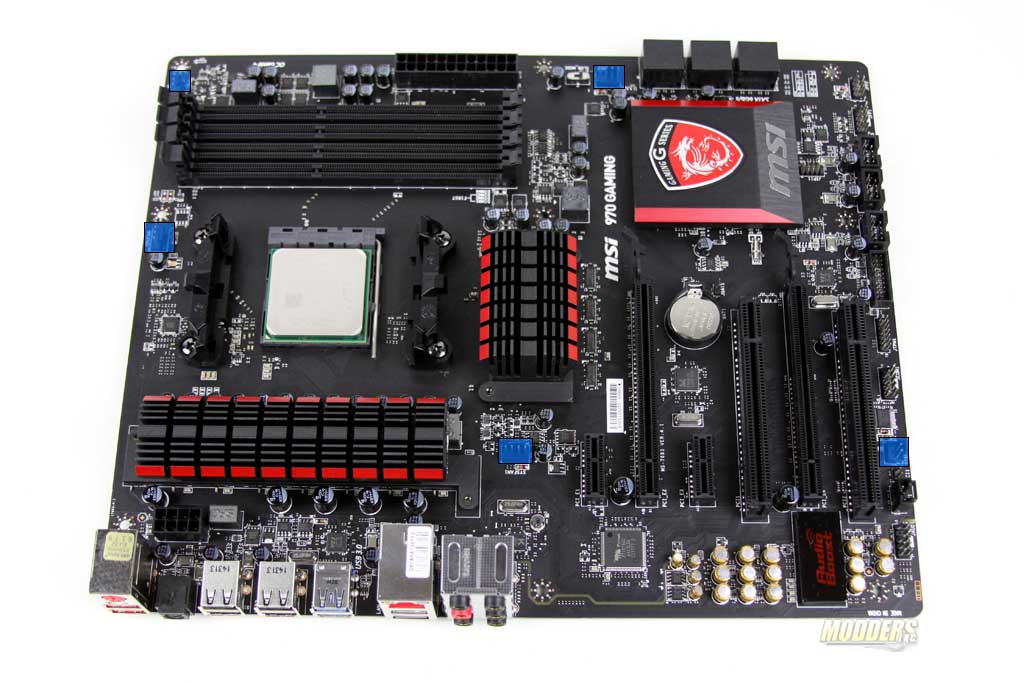
There are five fan headers in total, three of which are 4-pin (CPU, right edge and rear fan) and two are 3-pin (located at the top right and bottom edge) locations:
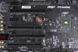
There are a pair of PCI-E x1, PCI-E x16 and PCI slots on the 970 GAMING motherboard spaced out for optimal multi-GPU breathing room. The expansion slot distribution from from top to bottom:
- PCI-E 2.0 x1 via 970 Chipset
- PCI-E 2.0 x16 via 970 Chipset
- PCI-E 2.0 x1 via 970 Chipset
- PCI via SB950
- PCI-E 2.0 x16 (8x electrical) via 970 Chipset
- PCI via SB950
 |
 |
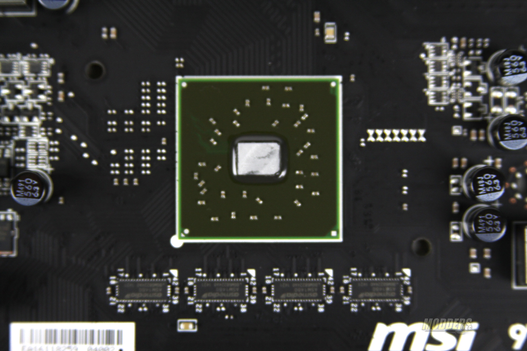
The spacing between the two PCI-E x16 slots is generous for reasons related to optimal dual-video card ventilation. Unlike other 970-chipset based mainboards, the MSI 970 GAMING is capable of 8x/8x PCI-E lane distribution via 3rd party ASMedia ASM1480 16-to-8 switches located right below the 970 Northbridge.
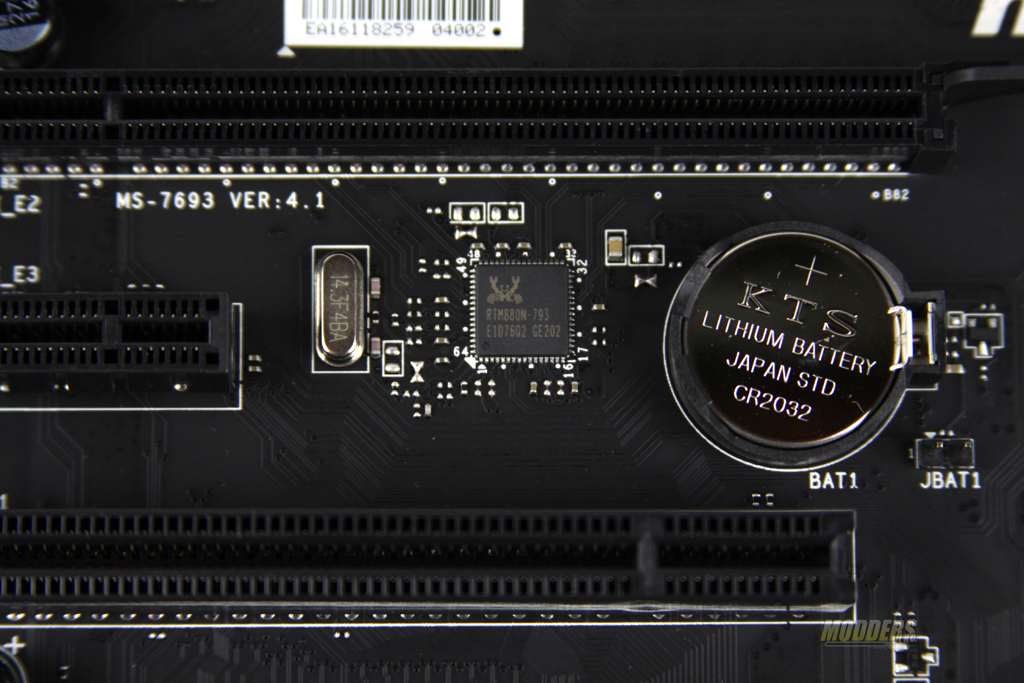
Right between the first PCI-E x16 slot and PCI slot sits a Realtek RTM880N-793 clock generator, controlling clock frequency for the host clocks of the motherboard. Right beside it is the CMOS battery and the clear CMOS jumper.
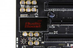
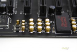
The “Audio Boost 2” solution on the MSI 970 GAMING uses a Realtek ALC1150 HD audio codec. The Audio Boost 2 area is isolated with separate grounding from the main PCB and the audio codec is covered to minimize interference. This area is also backlit with LEDs when the motherboard is powered on. There are also a pair of Texas Instruments OPA1652 amplifiers for the output and all the capacitors used are Nichicon MW series aluminum electrolytic caps.
 |
 |
 |
 |
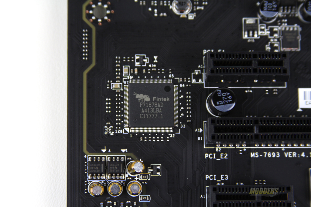
A Fintek F71878AD handles all the SuperIO functions including system monitoring.
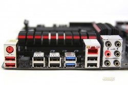
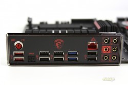
The rear IO provides a PS/2 port, eight USB 2.0 ports, a pair of USB 3.0 ports, six gold-plated audio ports and a Gigabit LAN port provided by a Qualcomm Killer E2205 Gigabit LAN controller. Since the AMD FX platform has no native USB 3.0 support, MSI turned to VIA with their VL806 host controller for a solution. A VL806 host controller takes an available PCI-E lane and provides a pair of USB 3.0 ports. One VL806 is used for the rear IO and another one is used for the 19-pin USB 3.0 header onboard. The red USB2.0 ports are MSI’s “Gaming Device Port”, introduced during the Intel Z77 chipset era. These ports have more gold content in their connectors to minimize oxidation.
 |
 |
