Intel Core i7-6700K Review: Inching Toward Extreme
Overclocking Behaviour
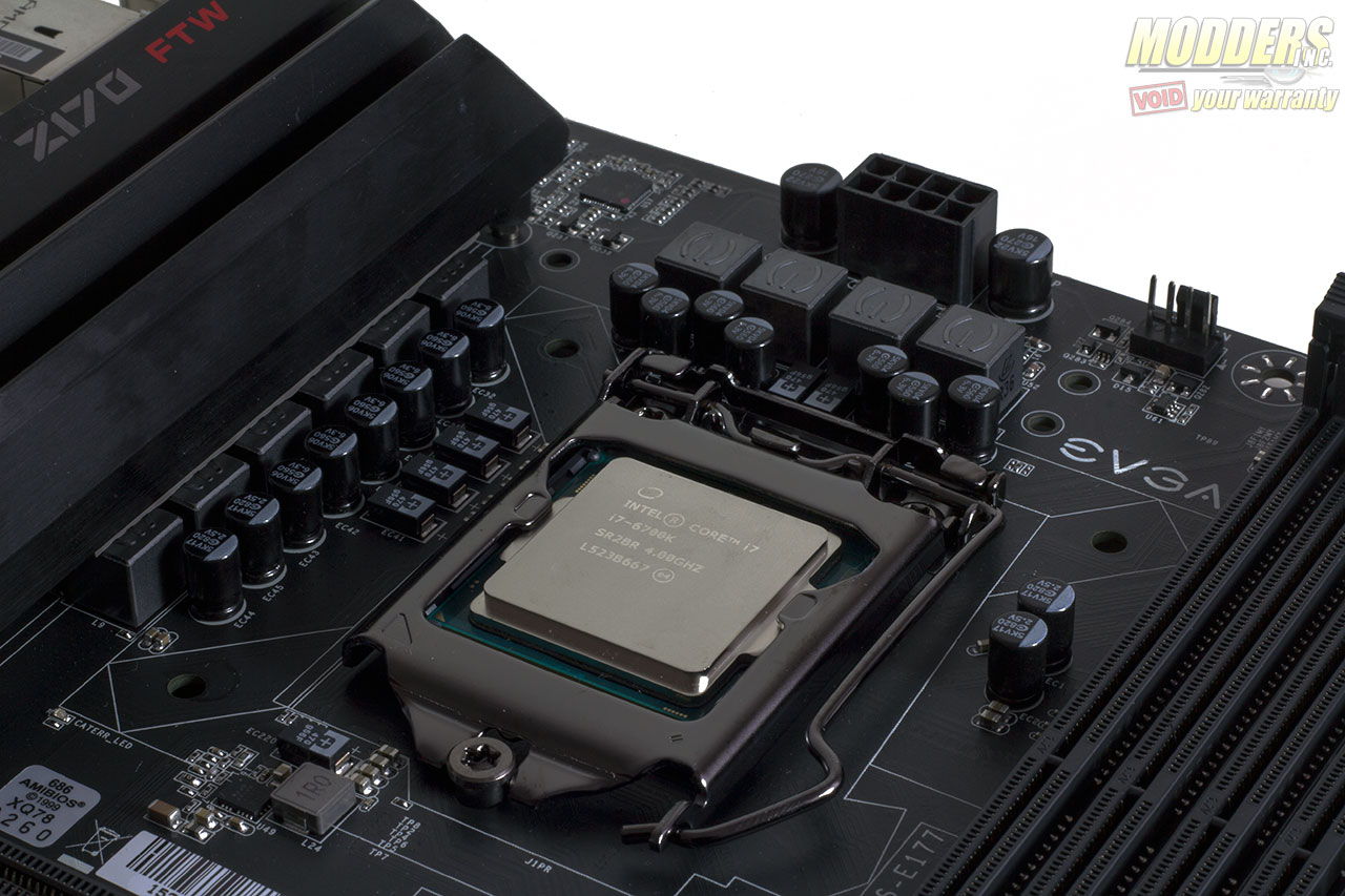
While overclocking remains as straightforward as before with unlocked processors, there are some notable changes on the Shark Bay platform compared to Z87 and Z97 which improves the overclocking experience once again. First, the voltage regulator has been moved off-die and is once again handled directly by the motherboard. Z87/Z97 used a fully-integrated voltage regulator (FIVR) which took a single input (VCCin) and distributed voltages to the CPU core, GT graphics, IO and System Agent. The good thing about FIVR is that even entry level Z87/Z97 motherboards could reach the same unlocked overclocks as high-end motherboards but the integrated VR also increased temperatures. Plus, most overclockers do not like handing off the control like that. Having FIVR also meant that real-estate was freed up on the motherboard (works well for ITX) and total component cost to manufacture the mainboard is less. On Z170 motherboards, CPU Core (VCCIA), IGP (VCCGT), System Agent (VCCSA) and IO (VCCIO) are four independent voltages fed separately from the motherboard. Designs will vary with overclocking oriented motherboards using new fully digital PWM controllers for all four while some boards will only worry about VCCIA and save cost on everything else. This puts the added component cost on motherboard manufacturers and down to the consumer as well but users regain more control. VRM component analysis will be explored as usual on the Z170 motherboard reviews following this article, like was done starting with the Z97 motherboard launch last year here at Modders-Inc.
Intel has not fully disclosed the new Skylake architecture yet but what is known and observable from the i7-6700K is that BCLK and DRAM overclocking have been improved. The relationship between BCLK and DMI is now different as BCLK is not tied down by straps and can be altered without affecting the other’s operating frequency. DRAM overclocking is also a lot more granular, allowing for 100/133MHz DDR4 ratio spacing. Memory overclocking will require more than just feeding DRAM voltage, System Agent and VCCIO have to be raised as well and are important if going for higher than 3000MHz overclock stability. I have more memory kits coming so this is something that will also be explored further with subsequent DDR4 reviews. The particular kit I used is a quad-channel kit that can handle much tighter timings but does not seem to be capable of much higher frequencies so you will have to get a rain check for the memory overclocking section. Cache can be overclocked separately as well in ratio form but none of my benchmarks show any noticeable performance even at 4.8GHz, at least on the test suite I currently employ.
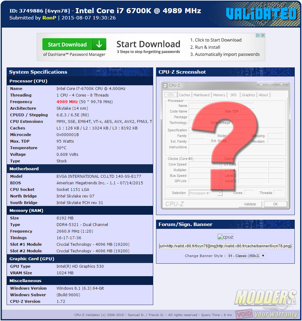
Overclocking on Skylake will be explored further in future articles, but a quick multiplier OC shows that this engineering sample can hit 5GHz validation with 2666MHz XMP profile loaded and using the integrated graphics. Voltage is not being detected correctly on this EVGA Z170 FTW motherboard by CPU-Z or AIDA64 at this version but Vcore was set to 1.4V. Even at 1.5V, this specific processor cannot successfully boot into Windows 8.1 completely at 5GHz.
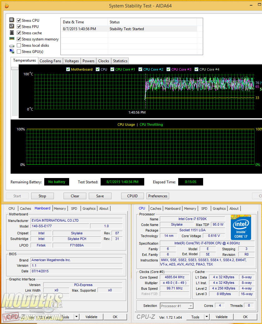
Highest 24/7 OC with a quick 15-minute AIDA64 stability test (same setting used on our heatsink reviews here at Modders-Inc) is 4.9GHz @ 1.36V. Users with custom liquid cooling systems will benefit the most from high overclocks and it is recommended as All-in-One liquid coolers and high-end air-coolers are bottlenecked by the temperatures even at 1.37V (the Vcore level in which this particular CPU throttles down as it reaches the max temperature compared to 1.36Vcore at 4.9GHz). Notes and specifics on how to overclock this i7-6700K will be shown on the EVGA Z170 Motherboard review following this article and on subsequent Z170 motherboard reviews that follow.
Power Draw and Temperatures
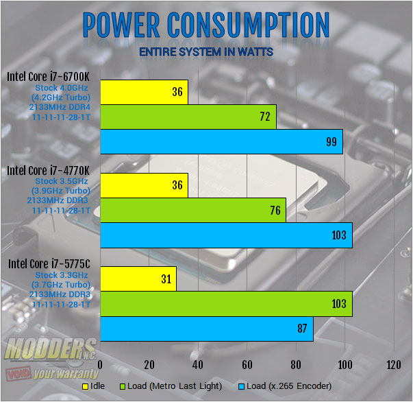
At stock, maximum temperatures at the hottest core reached 60C with the NH-D15. Overclocked to 4.9GHz (screenshot above), maximum core temperature without throttling within 15-minutes was 92C. (Moving voltage up to 1.37V would reach limit). Idle system load matched the i7-4770K but consumed less in both Metro Last Light and x.265 encoder loads. Despite having a higher TDP label than the i7-4770K and having higher frequencies at stock, the i7-6700K ran cooler and consumed less power.
Final Thoughts
This review arrives a few days late from the embargo date even though I had the CPU ready for a week before launch. I have only received my first Z170 motherboard the night before the morning embargo, so needless to say, I would not have had the time to properly test things as thoroughly as I would have wanted so apologies for for those waiting for a zero-day article. On the plus side, I got to test a whole bunch more than I normally would (some results of which will be in articles coming out later on) and assess the platform as a whole and put into perspective where this upgrade cycle fits in.
For an end user, all that is visible is the CPU’s performance with little care or knowledge of the difficulty involved in the manufacturing process that is barreling quickly towards the end of Moore’s Law. Spoiled by the massive leaps seen in Nehalem and Sandy Bridge, users have been wanting the same leap reproduced but this is pretty much never going to happen again unless something truly revolutionary technologically is discovered. This does not mean that the upgrade cycle has stopped but it does mean that the scenario has to be looked at beyond simply looking at benchmark numbers. For those simply looking for a blunt answer, NO, you do not need to upgrade to a Skylake CPU from a Haswell from a pure CPU benchmark standpoint. I would venture to say (even without having a benchmark ready) that a Sandy Bridge to Skylake upgrade would not be something to recommended, especially if it is primarily a gaming system. Also, as seen in the benchmark results above, Skylake discrete GPU framerates are showing lower numbers in some games compared to Haswell. Upgrading to Skylake and the new platform however does offer something unique that allows it to inch toward the extreme and it involves the Z170 chipset.
What I would argue is the real star of this show, the Z170 chipset makes up for the underwhelming change between the Z87 and Z97 chipset which added M.2 and SATA Express support. The Z170 chipset provides up to 20 PCI-E 3.0 lanes compared to Z87/Z97’s eight PCI-E 2.0. There are still no SATA Express products available in the market so I am probably going to stop talking about it as a feature for motherboards until that happens but current and upcoming M.2 products are very exciting otherwise. The PCI-E 2.0 lanes afforded by the Z97 PCH was not too impressive for what it was trying to do. As I discussed in my FX-9590 processor review last year, PCI-E 3.0 for graphics is not any close to being saturated so using those available lanes for storage makes the most sense, which is what ASRock has done with a lot of their Z97 motherboards, utilizing the CPU PCI-E 3.0 for Ultra M.2 connectivity. The lack of the rumoured PCI-E 4.0 for graphics in Z170 is not something that will be missed but the 20 lanes of PCI-E 3.0 via PCH and improved DMI (8 GT/s vs 5 GT/s in Z97) is a change that needs to be applauded. Considering Intel’s recent advancements with their SSD solutions, it will not be surprising if they have something big on the horizon in the storage front that will benefit strongly from this change in the chipset. RST support also arrives to this front, completely opening the doors for PCI-E RAID storage on a mainstream level. This is incredible performance potential for a mainstream platform.
The move back to non-FIVR CPUs is noted for its effort to court the overclockers back as well. I must admit that I did not see that coming at all, higher temperatures and hampering OC potential aside, the current implementation probably required some more reworking that is not ready for primetime yet on 14nm. Not that I am completely dismissing this as a ‘Marie Antoinette’ move on Intel’s part as considering how long it takes to bring a CPU to production, Intel was most likely aware of possible FIVR issues at 14nm long ago, even before enthusiasts complained about Haswell’s overclockability. The move back to a fully integrated voltage regulator is ultimately inevitable for Intel as it provides finer grain control and flexibility compared to motherboard VRMs, able to shift between power states much more quickly. It just makes more sense from a manufacturer standpoint as well because of the production scale across different devices so expect it to be back.
Skylake also marks DDR4’s entry to the mainstream desktop level. While introductory DDR4 prices scared many away, prices have dropped significantly with more affordable kits coming especially now that dual-channel modules are required for Intel’s LGA1151 motherboards. A single 4GB 2400MHz module fetches for ~$30 so two piece 8GB kits will cost around $60 (2666MHz modules start at $35 each). In comparison, a 4GB x2 2400MHz DDR3 memory module costs $55 so there is not much chasm between the two at the time of this article. This adds to the overall appeal of building on the new platform if assembling a system completely from the ground up compared to a Haswell/Devil’s Canyon/Broadwell based build as the price difference is minimal in the transition.
[sc:must_have_award ]

DDR3L refers to a set of specifications, most notably voltage, for DDR3 DIMMs including, but not limited to, SODIMMs. It’s not just for laptops, and it’s not just the small sticks.
Thank you very much. Information verified and article has now been updated.