Gigabyte GTX 980 G1 Gaming 4GB Video Card Review
Gigabyt GTX 980 G1 Gaming – Under The Hood
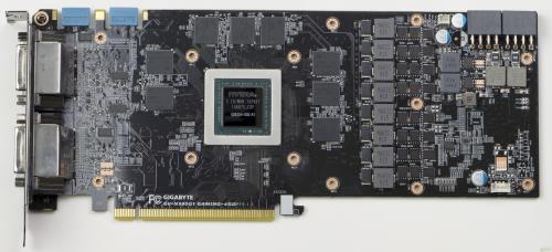 Pulling the Windforce 3x cooler and the backplate off of the GPU is extremely easy. A Phillips screw driver and a few screws later, both parts easily come off.
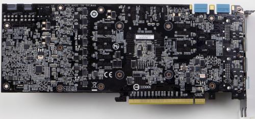
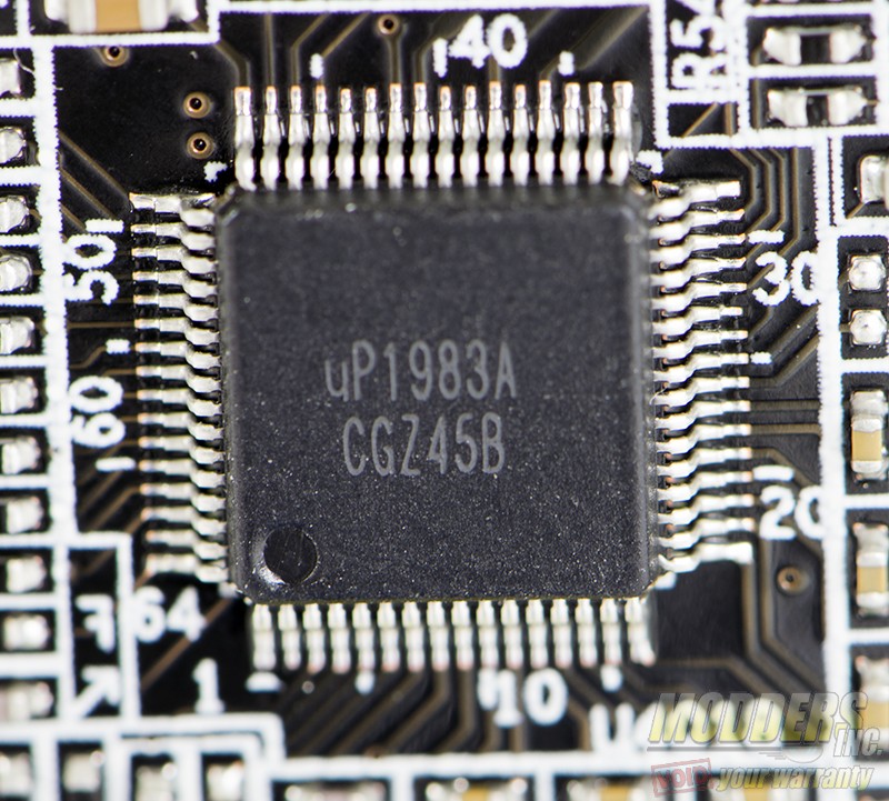
The Gigabyte GV-N980G1 Gaming-4GD video card has a customized 8+2 phase VRM compared to the reference GTX 980 which only utilizes a 4+1 design. The Texas Instruments INA3221 on the back edge is a 3-channel high-current bus and voltage monitor involved in power distribution. The largest chip at the back of the PCB is a UPI Semiconductor uP1983a which serves as the GPU PWM controller with three Reneses MOSFETs per phase on the other side: One RJK03B7DPA on the low-side and a pair of RJK0393DPA WPAK Power MOSFETs. Output filtering consists of 8x Magic Technologies 0.15uH SPRN surface mounted inductors and up to 20x 330uF Tantalum capacitors on the both sides of the PCB.
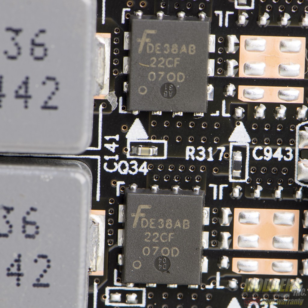
For the memory power delivery involves an On-semi NCP81172 dual-phase buck controller and a Fairchild FDMS3668S PowerTrench MOSFET per phase.
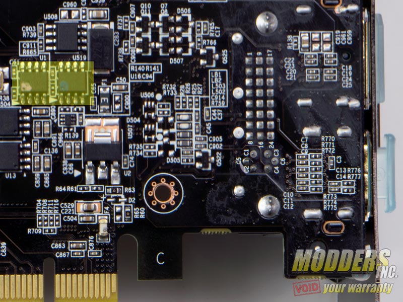
Gigabyte has outfitted the GTX 980 G1 Gaming with dual-bios in the back (marked in yellow in the photo) so there is redundancy fail-safe should the first one get corrupted, the card should still be able to boot.
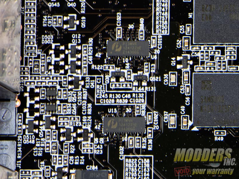
Tucked towards the rear connectors on the PCB these two Pericom PI3WVR 4-lane DP/HDMI switches, each capable of up to 5.4Gbps data rate transfers. These are responsible for the flexible display output capabilities of the GTX 980 Gaming G1.
