Gigabyte 990FXA-UD3 Rev 4.0 Motherboard Review: Old but Gold
A Closer Look at the Gigabyte 990FXA-UD3 Rev 4.0 Motherboard
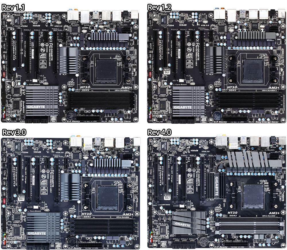
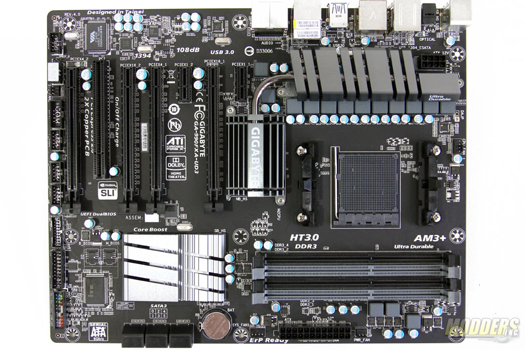
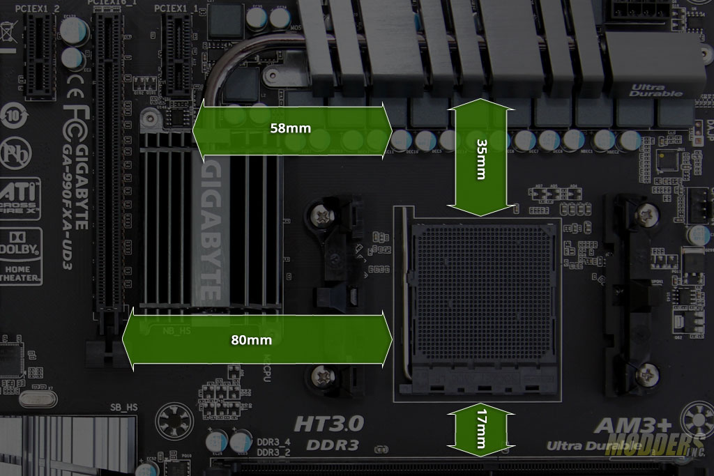
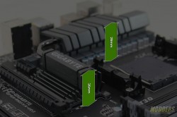
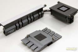
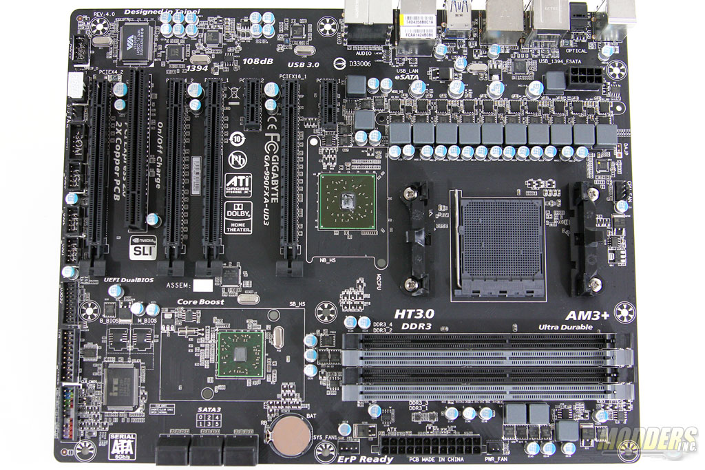
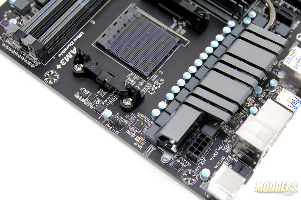
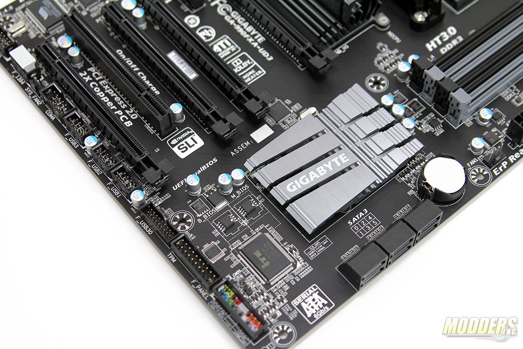
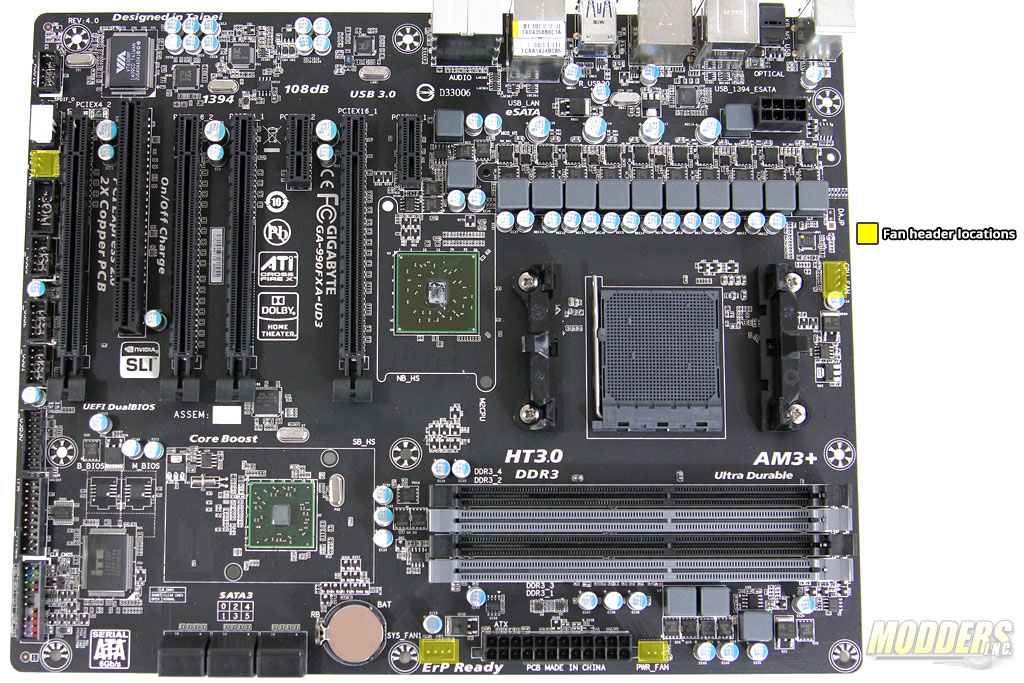
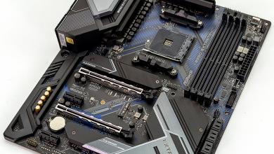
The Gigabyte 990FXA-UD3 Rev 4.0 motherboard uses a standard ATX form factor on a matte black 4-layer PCB. The most obvious change compared to previous revisions comes in the form of the heatsink design which is a little less sleek looking but is certainly a lot more functional with a large heatpipe connecting the CPU MOSFET heatsink to the north bridge. Not that the 990FX North Bridge needs it as it is has a 19.6W TDP rating but the CPU MOSFETs require as much cooling as it can get especially when running overclocked Bulldozer and Piledriver FX processors to prevent throttling. The chokes are also improved compared to the smaller Chiclet looking inductors on the previous revisions.
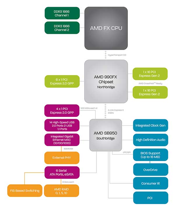
Before we proceed with the full layout, let us familiarize ourselves once again with the official AMD FX series block diagram illustrated below.
Unlike the FM2+ platform and recent Intel motherboards,990FX AM3+ motherboards have a separate 990FX North Bridge chipset with a 19.6W TDP and is essentially a PCI-E 2.0 switch providing up to 32 lanes for graphics which can be carved up into two x16 slots or up to four x8 slots which support both AMD CrossFire and NVIDIA SLI. Six additional x1 PCI-E lanes are available for other function as well for a total of 38 lanes. This North Bridge should not be confused with the CPU North Bridge that is built into the CPU itself which has its own clock domain and voltage plane for the memory controller and cache. In comparison, the FM2+ Kaveri platform has the PCI-E northbridge functions built into the APU. This is why you see AMD FX VRM explained in terms of 4+1 or 8+2 because it is referring to the main CPU voltage aka Core voltage aka Vcore aka VDD and the CPUNB voltage power aka VDDNB.
Thick thermal pads are used on the VRM MOSFETs while the 90FX North Bridge uses thermal compound and the SB950 South Bridge uses a thin thermal tape. All heatsinks are held in place through the back with spring-loaded screws and contact is very tight as it should be with no wobbling on the MOSFET heatsink. All heatsinks incorporate fewer angled airflow channels across their surface compared to the previous revision heatsinks which had a higher number of straight channels as they relied on active cooling from case air flow rather than just for size or via heatpipe. With the heatsinks removed we get a clear view of the important changes made on the 990FXA-UD3 Revision 4.
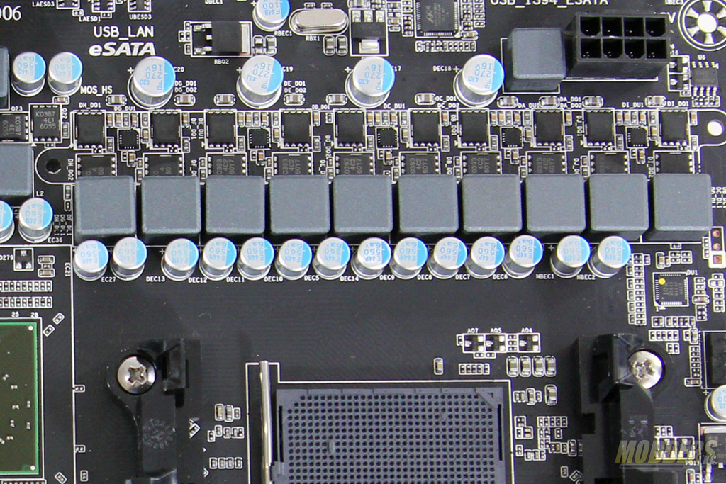
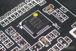
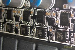
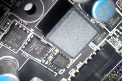
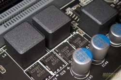
Input power goes through four 270uF input capacitors before 12V power is fed to the Renesas RJK0393DPA low side and RJK03B7DPA WPAK high-side MOSFETs (a total of 10 pairs). For the PWM controller, Gigabyte has moved on to using a fully digital International Rectifier IR3564B on the Revision 4.0, upgraded from the analog Intersil ISL6329 PWM controller of the Revision 3.0. This IR3564B is a 4+1 phase controller, fully supporting AMD SVI1 and SVI2 as well as Intel VR12 and VR12.5 specifications so you might see these in Intel motherboards as well. To get the 8+2 design, Gigabyte uses five IR3598 dual-MOSFET drivers configured as an interleaved doubler to drive the two pairs of Renesas WPAK MOSFETs flanking it. Ten 0.68uH inductors together with 14 560uF solid capacitors make up the output filter.
The 8-pin CPU power is located as right along the top corner overhang of the MOSFET heatsink at a 90 degree angle.
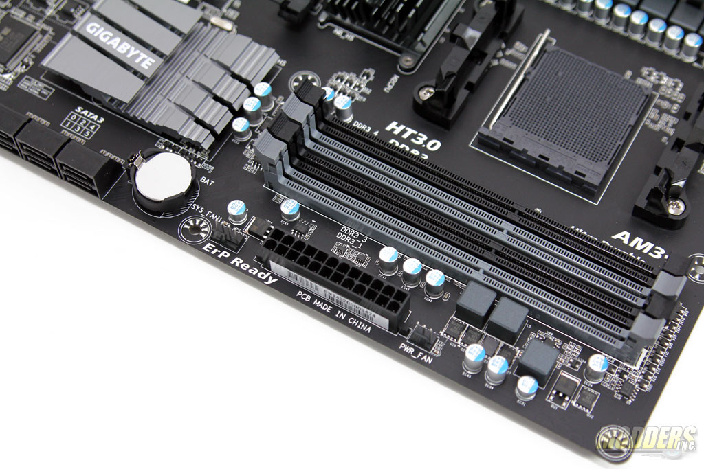
A Richtek RT8120D is used with two chokes and two pairs of Renesas RJK03B7DPA MOSFETs for the 990FX chipset as well as for the memory power (DRAM uses an RT9199 for termination voltage). The four dual-channel DIMM slots alternate in black and gray colors per channel and supports up to 32GB of DDR3 memory at 2133MHz (up to 10.66 memory multiplier via UEFI).
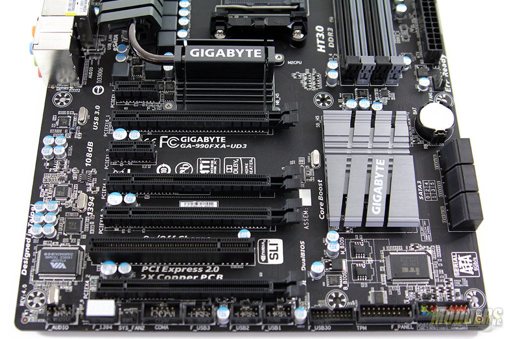
Six SATA3 6G ports are natively provided by the AMD SB950 chipset and are at a 90 degree angle on the edge for maximum graphics card clearance. The front panel connectors in the corner are color coded with polarity marking and labels for easier installation inside a case. Directly above it are two open pins used to reset the CMOS. Users simply short this connector (when the system is turned off and not plugged in) with any metal for a few seconds to reset CMOS. A Trusted Platform module is also available right beside it.
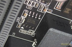
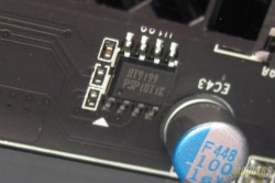
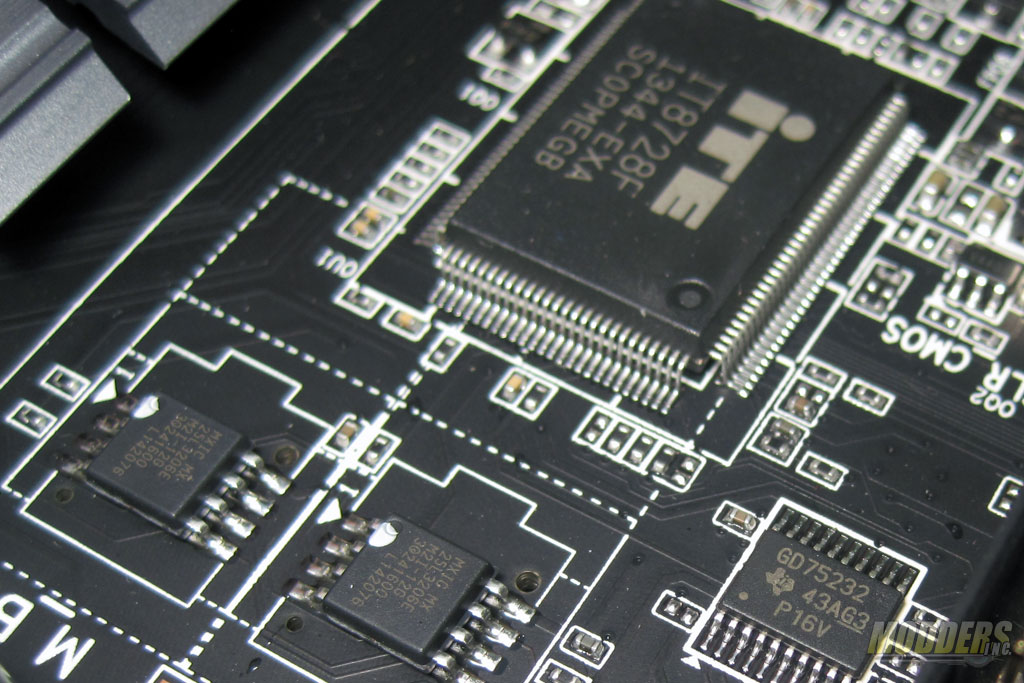
Below the SB950 South bridge are two MXIC 25L3206E 32Mbit flash memory chips, one contains the main BIOS while the other is for redundancy so the system can recover in case of corruption and continue booting without the need for RMA. Right beside the BIOS memory, there is an ITE IT8728F Super-IO controlling many features including PWM fan speed control, serial port and hardware monitoring.
The 19-pin USB 3.0 front panel header at the bottom edge and two USB 3.0 ports are provided by a 3rd party VIA VL805 controller, taking one PCI-E x1 lane from the 990FX chipset and producing four total downstream outputs. The AMD SB950 chipset provides a maximum of 14 USB 2.0 ports natively and all of these are implemented on the GA-990FXA-UD3 with three 9-pin USB 2.0 headers at the bottom edge for front panel or rear expansion slot connectors and eight USB 2.0 ports in the rear IO. A VIA VT6308P IEEE 1394 “Firewire” host controller provides an onboard header via the AMD SB950 PCI interface with two downstream ports with data speeds of up to 400 Mbps. One is provided from the onboard header and the second port is provided directly via the rear IO. For some reason this is the only onboard header with a cover on it on the 990FXA-UD3 Rev 4.0.
Expansion slots from top to bottom:
- PCI-Express x1 (via SB950)
- PCI-Express x16 (via 990FX)
- PCI-Express x1 (via SB950)
- PCI-Express x16 (only x4 electrical via 990FX)
- PCI-Express x16 (via 990FX)
- PCI slot (natively via SB950)
- PCI-Express x16 (only x4 electrical via 990FX)
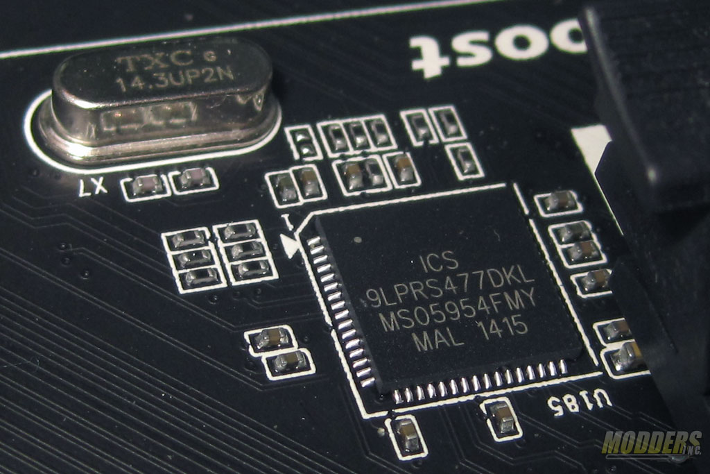
Right between the expansion slots and the SB950 chipset is an ICS 9LPRS477DKL clock generator, controlling clock frequency for the host clocks of the motherboard.
There are four fan headers in total. The 4-pin CPU_FAN header and 4-pin SYS_FAN headers are PWM controllable. A 3-pin PWR_FAN is located on the edge flanking the 24-pin CPU power connector with the first SYS_FAN. A secondary SYS_FAN is located at the bottom edge towards the rear and is also a 3-pin header.
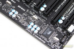
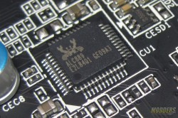
For the audio subsystem, Gigabyte uses a Realtek ALC889 CODEC supporting 7.1 + 2 channel playback (rear + front panel) with 108dB SnR DAC and 104dB SnR ADC.
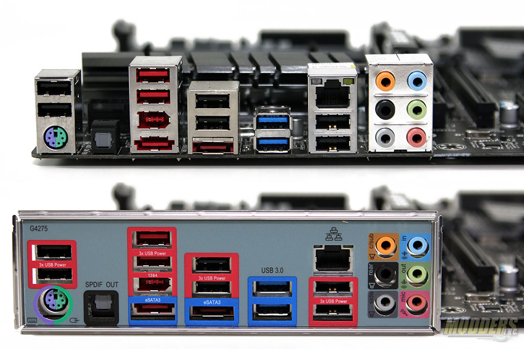
The rear IO has a color coded and labeled shield outlining the previously mentioned USB 2.0 ports (all of which feature Gigabyte’s 3X USB power), USB 3.0 ports via the VIA VL805 controller and analog audio ports with an optical SPDIF out. A PS/2 port is provided by the Super IO chip for legacy keyboards and mice.
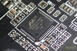
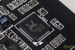
A pair of External SATA ports are provided by a Marvell 88SE9172 host controller taking one PCI-E x1 lane and providing the two SATA3 6Gb/s ports. The LAN controller used is a Realtek RTL8111F, providing Gigabit LAN connectivity supporting jumbo frame to 9K bytes and Wake-on-LAN as well as remote wake-up functions.
