(Almost) Everything You Need to Know About the New AMD Radeon 300 Series Line-up
CEO Lisa Su and the AMD crew had a major announcement at E3, promising to “usher a new era” of PC gaming with their latest 300-series graphics cards. Understandably, you probably do not have time to watch the entire event so I have watched it for you and summarized, simplified and explained what the announcement covered below. With NVIDIA’s recent announcement of the GTX 980Ti, pricing AMD’s new flagship “Fury X” video card is crucial and it seems that they have succeeded in that but that is of course, just part of the story. First, below is a breakdown of the announced cards and their prices:
| AMD Radeon™ R9 and R7 series GPU Model | PRICE | Memory | Release Date |
|---|---|---|---|
| AMD Radeon™ R9 Fury X | $649USD | 4GB HBM | June 24 |
| AMD Radeon™ R9 390X | $429USD | 8GB GDDR5 | June 18 |
| AMD Radeon™ R9 390 | $329USD | 8GB GDDR5 | June 18 |
| AMD Radeon™ R9 380 | $199USD | 2GB, 4GB GDDR5 | June 18 |
| AMD Radeon™ R7 370 | $149USD | 2GB, 4GB GDDR5 | June 18 |
| AMD Radeon™ R7 360 | $109USD | 2GB GDDR5 | June 18 |
Other models:
- Radeon R9 Fury (non-X): $549 USD with July 14th release date. Full specification forthcoming.
- Radeon R9 Fury Nano: Small-form factor. No price or firm release date (sometime in the summer).
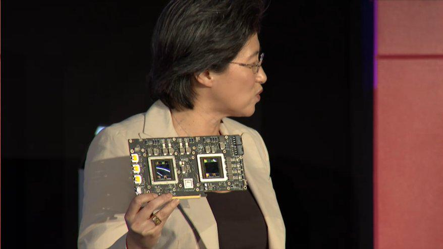
- Radeon R9 Dual Fury X: No official name yet (photo below, courtesy of PC Gamer’s twitter @PCgamer).
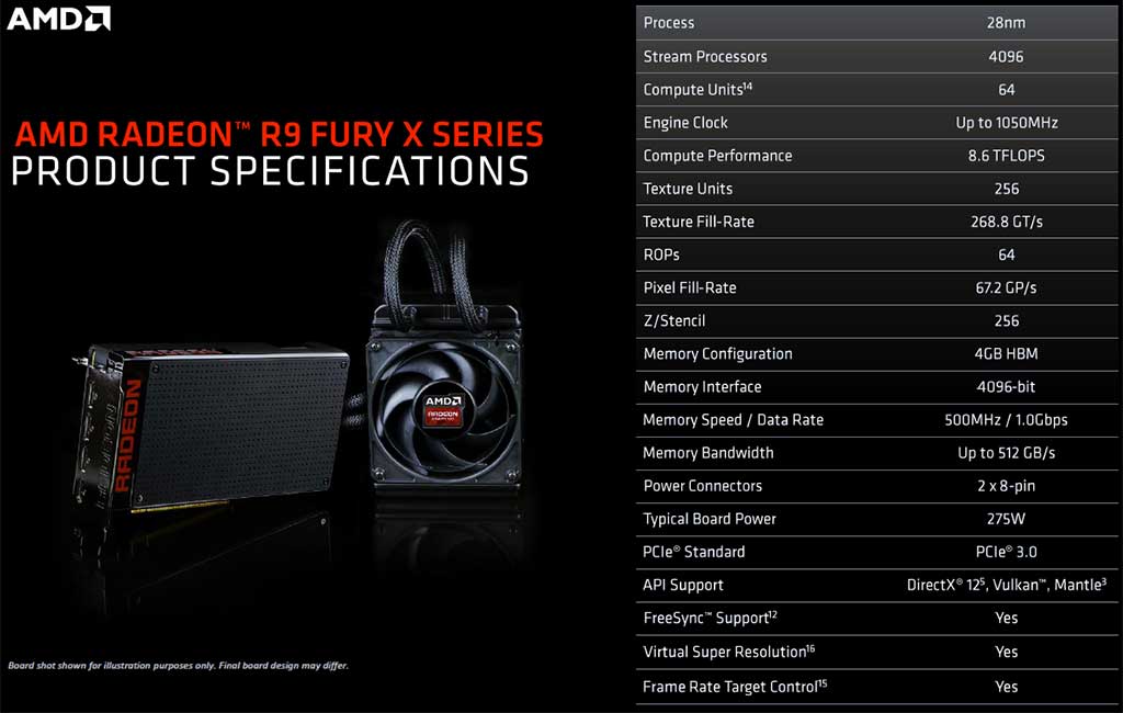
From the official specifications of the Radeon R9 Fury X, it is interesting to see that despite the higher performance some numbers on Fiji are lower, including the smaller PCB size enabling the NANO version and the dual-GPU that is not as ridiculously long as older AMD dual-graphics video cards. Fiji is built using the same, albeit more mature 28nm process and has smaller memory at only 4GB. This is of course High-Bandwidth Memory (HBM) not GDDR5 which is a game changer entirely (4096-bit memory bus! compared that to 512-bit). The TDP is also surprisingly, slightly lower than the R9 290X (275W vs 290W).
Re-brand or Not?
Looking at the charts above we can quickly analyze what is going on. We are going to separate the truly next-gen cards (referred to as “Fiji”) from the other R9/R7 models utilizing GDDR5 (referred to as “Carribean Islands” cards). While the Carribean Island cards are still utilizing GDDR5 instead of HBM (High-Bandwidth Memory), AMD has reworked and optimized the micro-controllers within the ASIC to squeeze more processing power, coupled with a more mature manufacturing process that will allow the “rebranded” cards to perform better at the same TDP as their 200 series equivalents, and more importantly at the same price. This is not too dissimilar to when NVIDIA re-branded their 600 series to 700 series cards. At least AMD kept the naming scheme the same with the 300 series equivalent cards having the same naming scheme as the previous 200 series cards which should avoid some level confusion. These cards will also be DirectX12, Vulkan, Mantle and Open GL 4.5 API compatible.
“Full DX12 Support?”
The DirectX 12 API has been designed to work with current existing hardware, requiring only Windows 10, tiled resources, and virtual memory but obviously certain features will not be enabled depending on the hardware. The performance leap in DX12 should be massive and unlike DX11 which is heavily GPU dependent, the CPU is very relevant again if the developer manages resource properly. Prior to DX12, every single DirectX improvement is tied directly to a physical hardware upgrade but that is no longer the case giving more users a chance to enjoy the graphical upgrade. There has been a lot of confusion on what involves “full” hardware support however with both NVIDIA and AMD supporters spinning the hype to declare their side has it. Unlike NVIDIA, AMD is the only company that offers DirectX 12 tier 3 resource binding and asynchronous shaders for all their Graphics-Core Next (GCN) video cards. Even NVIDIA’s Maxwell only offers tier 2 (and their older Fermi at tier 1 with Intel Haswell/Broadwell). Resource binding is the process of linking resources (textures, vertex buffers, index buffers, etc), to the graphics pipeline, enabling the shaders of the pipeline to process the correct resource. Those classified in tier 1, are the most restrictive when it comes to the process while tier 3 are free from these limitations.
As for asynchronous shaders, this allows the AMD Radeon cards to manage the workload much more effectively having the ability to place tasks in separate queues instead of just a single queue in a pre-determined order. AMD made a video that simply explains what this means to the end user:
As for NVIDIA, only their latest iteration of Maxwell (GM20X) is capable of mixed queues with Kepler, Fermi and the first Maxwell cards only able to have a single graphic cue. NVIDIA’s claim of “full” DX12 support however is due to having higher feature level support over AMD video cards (DX12 Feature Level 12_1 vs 12_0). This specifically involves Rasterizer Order Views (ROV), enabling advanced blending functions and more advanced applications. Even AMD’s Fiji hardware does not have this capability. Rendering transparency, translucency and semi-opaque 3D items on the screen is troublesome when they are layered on the 2D screen. This can be anything from vegetation, glass, smoke, etc. ROV enables the underlying Order Independent Transparency (OIT) algorithms to use features of the hardware to try to resolve the transparency order correctly. Performance result would mean higher framerate and depending on implementation, better graphics. This is of course, is conditional and developer dependent. Some games may implement it and rely heavily on it while others won’t. Knowing NVIDIA’s modus operandi and the existence of NVIDIA GameWorks however, you can be sure that they will pour considerable resource into making sure as many AAA games as possible are implementing the features that are not available on AMD. Whether this is good or bad, I will leave it up to you, the readers to decide.
HBM and Why it is Game Changing
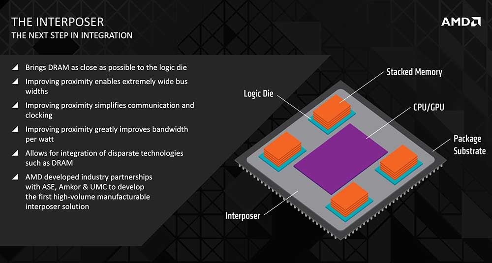
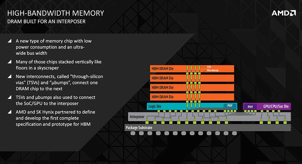
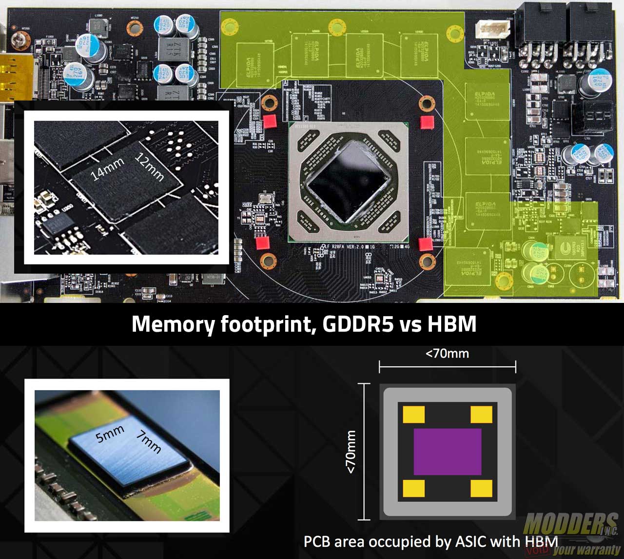
Coinciding with AMD’s announcement was SKHynix’ press release on ramping up HBM manufacturing on the same day. AMD and SKHynix have been developing High-Bandwidth Memory for some time now and have anticipated the upcoming bottleneck that GDDR5 memory power presents as GPU efficiency increases. In a typical video card, the set TDP includes memory power consumption as well and the more efficient the GPU gets, the memory takes up a larger fraction of that TDP. To solve this problem, HBM is integrated directly into the logic die, as close as possible to the processor. This minimizes latency, lowers power consumption, increases memory bandwidth, and frees up the PCB space since the VRM is simplified. SKHynix developed the stacked memory design to be able to fit the memory on such a small space while AMD developed the through-silicon vias (TSV) to interface the memory stack as well as the silicon interposer that routes the memory signal to the processor core. This is quite an incredible engineering feat considering the entire stack is only 100 microns thick.
GDDR5 vs HBM footprint comparison in yellow:
Four stacks of HBM is 4GB of memory with 1GB per stack and AMD claims that this is not going to be an issue because of the wider bus width (32-bit vs 1024-bit, per chip vs per stack). Although clock speed is slower at 500MHz compared to GDDR5 which can reach up to 1750MHz, total bandwidth on HBM can be greater than 100GB/s per stack compared to the 28GB/s per chip limitation of GDDR5. Because of the savings and performance implication of this technology, expect it to show up in more than just graphics card in the near future.
Also, other than that, AMD is betting on Virtual Reality, has framerate target control similar to what NVIDIA has implemented on their card last generation, VSR support similar to the AMD Tonga and newer cards, and all other information you can get at the Radeon R9 product landing page: http://www.amd.com/en-us/products/graphics/desktop/r9#. No reviews are out at the time of announcement unlike other major releases (essentially a “paper launch”, AMD instead opted to demonstrate the new video card performance to fans directly at a closed event. Reviews will be forthcoming however once retail availability hits.
