ADATA XPG Dazzle 2800MHz CL17 2x8GB DDR4 Review: Razzle-Dazzle Without The Hassle
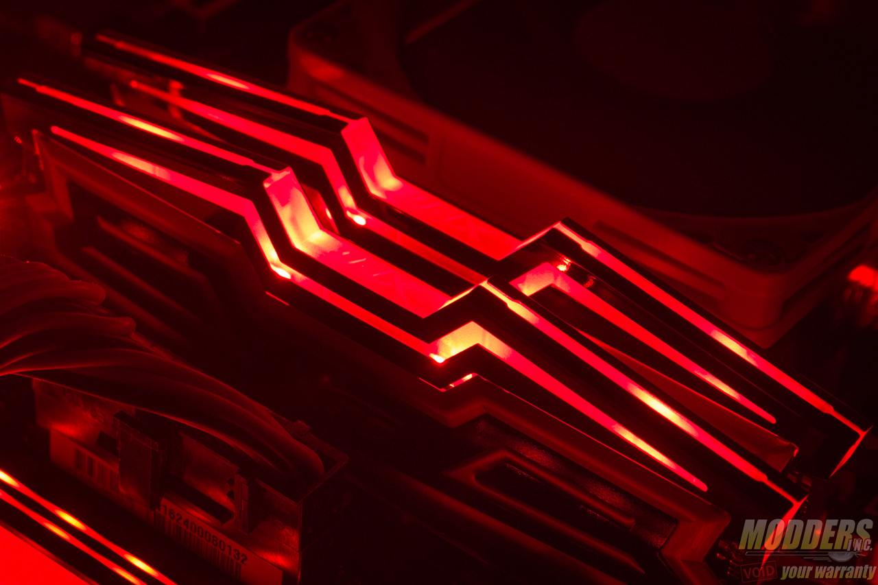
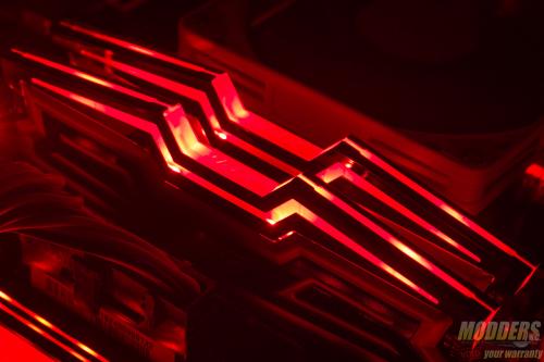
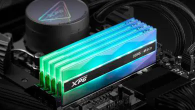
Available from 2400 through 3000 MHz dual or quad-channel kits, the ADATA XPG Dazzle DDR4 memory modules shines quite literally. Equipped with embedded LEDs on the PCB as developed by AVEXIR technology, ADATA’s XPG Dazzle glows to fit the increasing aesthetic demands of modders and system builders who are quite particular about how their system looks. As expected from a DDR4 kit, the XPG Dazzle comes with a lifetime warranty and is XMP 2.0 compatible for quick frequency and timing profile loading on Intel-based systems without a hassle.
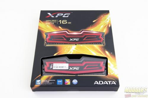
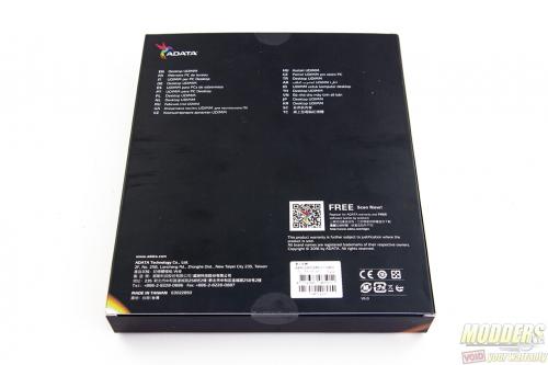
ADATA uses the same packaging with their dual-channel kits and quad-channel kits so it is quite sizable compared to typical memory modules. At the front is a preview window showcasing one of the XPG Dazzle memory while the back does not have the specifications listed but simply has the word “Desktop UDIMM” translated to 20 different languages.
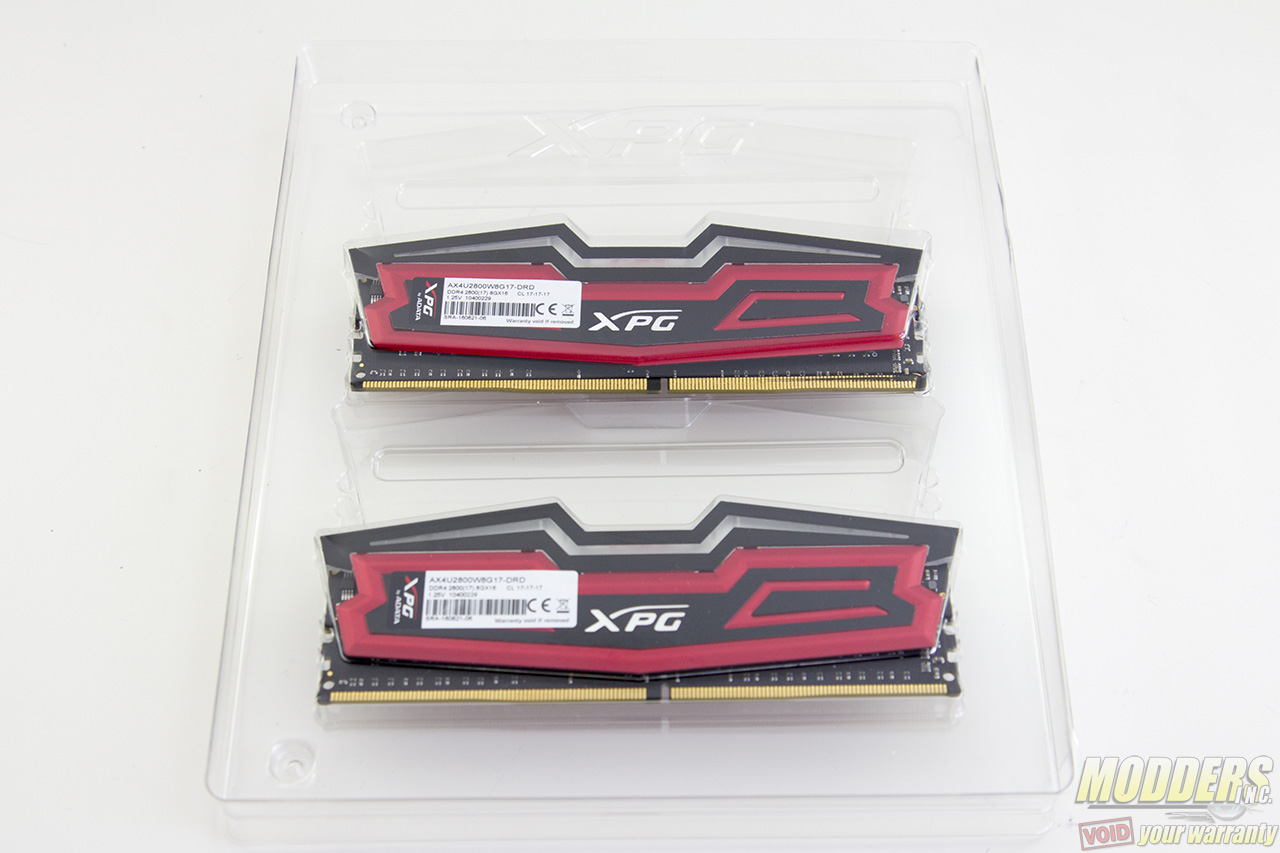
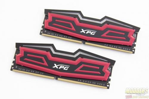
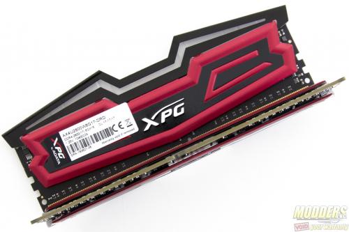
Each ADATA XPG Dazzle module measures 7.6mm x 138.9mm x 47.8mm, factoring in heatspreader. It is slightly taller, slightly thicker and slightly longer than a typical DDR4 module. The sticker shows the default XMP profile on this module at CL17-17-17 with 1.25V, surprisingly lower voltage than most even with additional lighting.
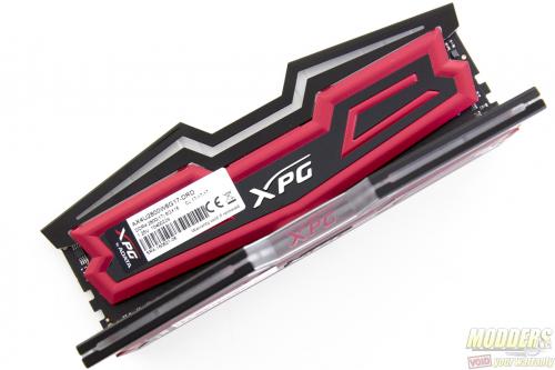
The heatspreader is a two-piece aluminum anodized black with red accents. The actual PCB itself just measures 30.8mm but the diffuser for the LED located along the top edge extends the height of the module.
Looking from the bottom reveals that the 8GB module is dual-sided and Thaiphoon Burner reveals them to be SK Hynix H5AN4G8NMFR chips in 512 x 8 configuration per side on a black PCB.
The EEPROM containing the SPD and XMP data is located at the edge, peeking out at the corner (unlike typical DDR4 modules with the EEPROM at the center) and here are some of the relevant information extracted from inside (via Thaiphoon Burner):
| Module Manufacturer: | A-DATA Technology |
| Module Part Number: | DDR4 2800 |
| DRAM Manufacturer: | Hynix |
| DRAM Components: | H5AN4G8NMFR-TFC |
| Module Manufacturing Date: | Week 25, 2016 |
| Module Manufacturing Location: | Unknown: 00h |
| Module Serial Number: | 00000000h |
| Lot Number: | 2201275701-X40091 |
| Module PCB Revision: | 00h |
| DRAM Stepping: | Undefined |
| Fundamental Memory Class: | DDR4 SDRAM |
| Module Speed Grade: | DDR4-2133 |
| Base Module Type: | UDIMM (133.35 mm) |
| Module Capacity: | 8192 MB |
| Reference Raw Card: | B0 |
| Initial Raw Card Designer: | Micron Technology |
| Module Nominal Height: | 31 < H <= 32 mm |
| Module Thickness Maximum, Front: | 1 < T <= 2 mm |
| Module Thickness Maximum, Back: | 1 < T <= 2 mm |
| Number of DIMM Ranks: | 2 |
| Address Mapping from Edge Connector to DRAM: | Mirrored |
| DRAM Device Package: | Standard Monolithic |
| DRAM Device Package Type: | 78-ball FBGA |
| DRAM Device Die Count: | Single die |
| Signal Loading: | Not specified |
| Number of Column Addresses: | 10 bits |
| Number of Row Addresses: | 15 bits |
| Number of Bank Addresses: | 2 bits (4 banks) |
| Bank Group Addressing: | 2 bits (4 groups) |
| DRAM Device Width: | 8 bits |
| Programmed DRAM Capacity: | 4 Gb |
| Calculated DRAM Capacity: | 4 Gb |
| DRAM Page Size: | 1 KB |
| Primary Memory Bus Width: | 64 bits |
| Memory Bus Width Extension: | 0 bits |
| DRAM Post Package Repair: | Supported |
| Soft Post Package Repair: | Not supported |
| Fine Timebase: | 0.001 ns |
| Medium Timebase: | 0.125 ns |
| CAS Latencies Supported: | 9T, 11T, 12T, 13T, 14T, 15T, 16T |
| DRAM Minimum Cycle Time: | 0.937 ns |
| DRAM Maximum Cycle Time: | 1.500 ns |
| Nominal DRAM Clock Frequency: | 1067.24 MHz |
| Minimum DRAM Clock Frequency: | 666.67 MHz |
| CAS# Latency Time (tAA min): | 13.500 ns |
| RAS# to CAS# Delay Time (tRCD min): | 13.500 ns |
| Row Precharge Delay Time (tRP min): | 13.500 ns |
| Active to Precharge Delay Time (tRAS min): | 33.000 ns |
| Act to Act/Refresh Delay Time (tRC min): | 46.500 ns |
| Normal Refresh Recovery Delay Time (tRFC1 min): | 260.000 ns |
| 2x mode Refresh Recovery Delay Time (tRFC2 min): | 160.000 ns |
| 4x mode Refresh Recovery Delay Time (tRFC4 min): | 110.000 ns |
| Short Row Active to Row Active Delay (tRRD_S min): | 3.700 ns |
| Long Row Active to Row Active Delay (tRRD_L min): | 5.299 ns |
| Long CAS to CAS Delay Time (tCCD_L min): | 5.355 ns |
| Four Active Windows Delay (tFAW min): | 21.000 ns |
| Maximum Active Window (tMAW): | 8192*tREFI |
| Maximum Activate Count (MAC): | Unlimited MAC |
| DRAM VDD 1.20 V operable/endurant: | Yes/Yes |
| Module Thermal Sensor: | Not Incorporated |
| SPD Revision: | 1.0 |
| SPD Bytes Total: | 512 |
| SPD Bytes Used: | 384 |
| SPD Checksum (Bytes 00h-7Dh): | CDEAh (OK) |
| SPD Checksum (Bytes 80h-FDh): | 27DEh (OK) |
| JEDEC DIMM Label: | 8GB 2Rx8 PC4-2133-UB0-10 |
| FREQUENCY | CAS | RCD | RP | RAS | RC | RRDS | RRDL | CCDL | FAW |
|---|---|---|---|---|---|---|---|---|---|
| 1067 MHz | 16 | 15 | 15 | 36 | 50 | 4 | 6 | 6 | 23 |
| 1067 MHz | 15 | 15 | 15 | 36 | 50 | 4 | 6 | 6 | 23 |
| 933 MHz | 14 | 13 | 13 | 31 | 44 | 4 | 5 | 5 | 20 |
| 933 MHz | 13 | 13 | 13 | 31 | 44 | 4 | 5 | 5 | 20 |
| 800 MHz | 12 | 11 | 11 | 27 | 38 | 3 | 5 | 5 | 17 |
| 800 MHz | 11 | 11 | 11 | 27 | 38 | 3 | 5 | 5 | 17 |
| 667 MHz | 9 | 9 | 9 | 22 | 31 | 3 | 4 | 4 | 14 |
| Profiles Revision: 2.0 | ||
| Profile 1 (Certified) Enables: Yes | ||
| Profile 2 (Extreme) Enables: No | ||
| Profile 1 Channel Config: 2 DIMM/channel | ||
| XMP PARAMETER | PROFILE 1 | PROFILE 2 |
|---|---|---|
| Speed Grade: | DDR4-2802 | N/A |
| RAM Clock Frequency: | 1401 MHz | N/A |
| Module VDD Voltage Level: | 1.25 V | N/A |
| Minimum DRAM Cycle Time (tCK): | 0.714 ns | N/A |
| CAS Latencies Supported: | 17T,16T,15T,11T | N/A |
| CAS Latency Time (tAA): | 17T | N/A |
| RAS# to CAS# Delay Time (tRCD): | 17T | N/A |
| Row Precharge Delay Time (tRP): | 17T | N/A |
| Active to Precharge Delay Time (tRAS): | 36T | N/A |
| Active to Active/Refresh Delay Time (tRC): | 53T | N/A |
| Four Activate Window Delay Time (tFAW): | 28T | N/A |
| Short Activate to Activate Delay Time (tRRD_S): | 5T | N/A |
| Long Activate to Activate Delay Time (tRRD_L): | 7T | N/A |
| Normal Refresh Recovery Delay Time (tRFC1): | 365T | N/A |
| 2x mode Refresh Recovery Delay Time (tRFC2): | 225T | N/A |
| 4x mode Refresh Recovery Delay Time (tRFC4): | 155T | N/A |
