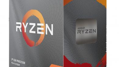
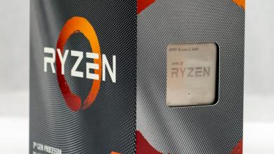
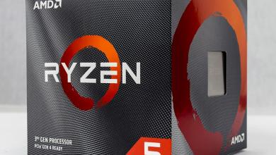
AMD Ryzen 7 3700X and AMD Ryzen 9 3900X CPU Review
Is this what we have been waiting for?
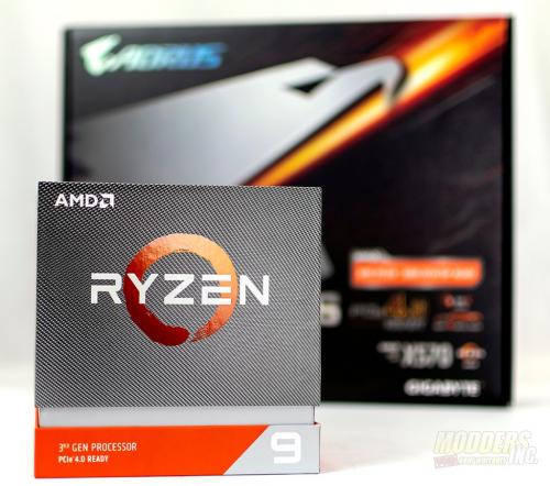
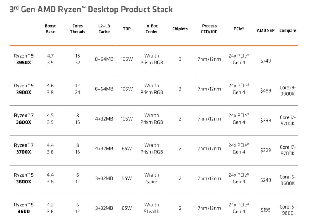
At CES 2019, AMD showed off some early silicon and introduced its 1st 7nm CPU. The AMD Ryzen 3000 series is now a reality. The new Ryzen 3000 CPUs move away from a monolithic core design and instead use a chiplet design. The idea is to have 7nm chiplets connected to a 12nm I/O die. The I/O die handles things like USB, PCIe for storage, and the memory controllers. Separating the CPU cores from the I/O allows AMD to increase yields and lower costs. A few architectural changes get thrown in as well. The new process shrink to 7nm and the generational changes to the Zen cores all lead to what AMD claims is a 15% increase in IPC. The two CPUs featured in this review is the Ryzen 9 3900x and the Ryzen 7 3700x. The Ryzen 9 series is new for this generation and features more cores. The Ryzen 9 3900X is a 12 core/24 thread CPU and features a 3.8 GHz base clock with a 4.6 GHz boost clock. The Ryzen 7 3700X is the replacement for the last generation flagship CPU, the Ryzen 7 2700X. The Ryzen 7 3700X retains the 8 core/16 thread configuration and features a 3.6 GHz base clock and a 4.4 GHz boost clock. AMD also updated the memory controller on Ryzen 3rd Gen to handle a much more diverse range of modules. Official transfer rates supported are 3200 MHz.
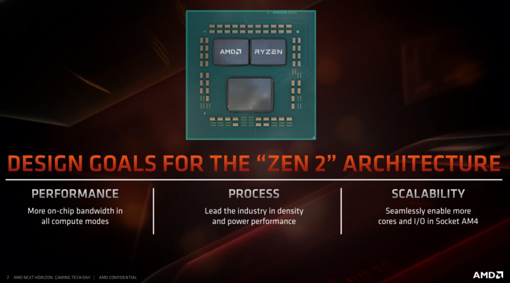
AMD Ryzen 3rd Gen or Zen 2, changes things up a bit. AMD’s design goals were to get more bandwidth between nodes, increase density while reducing power consumption, and enable more cores on the AM4 platform.
Below, we’ll go over a brief overview and hit the highlights. This is in no way meant to be a deep dive into the new Ryzen CPU architecture.
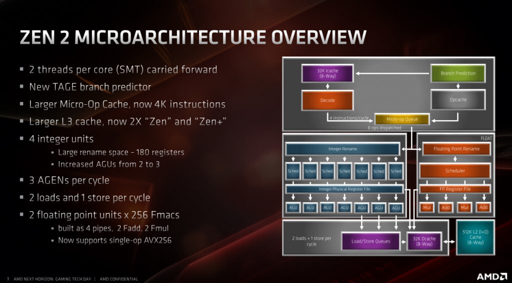
So how did they do it? SMT or Simultaneous Multi-Threading was carried forward from the previous generation. A new TAGE predictor was added. AMD improved the load/store bandwidth that keeps more data on-chip and increased throughput. A Larger 180 entry register files provide the CPU more access to more available working data.
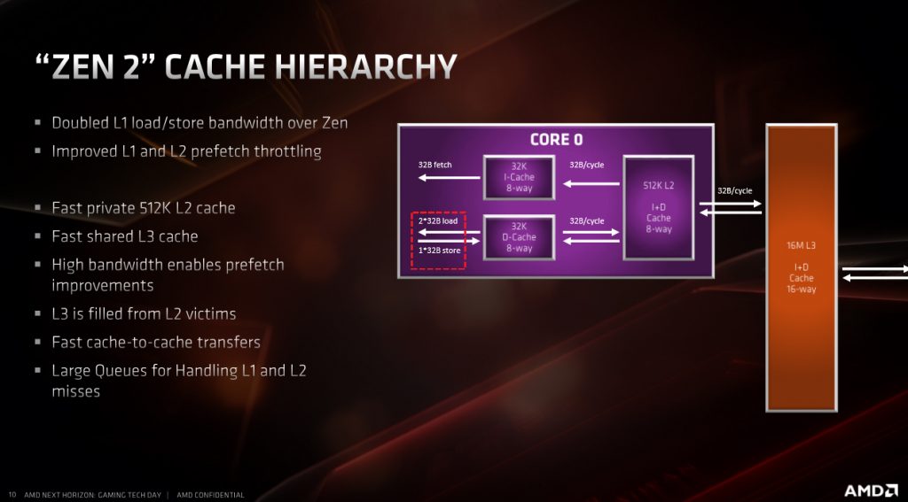
Cache is one of the biggest contributors to performance. AMD Doubled the L1 cache over the previous Zen architectures. L3 cache is doubled per CCD to 23 MB.
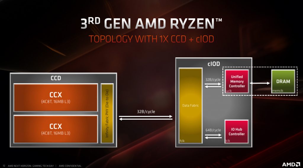
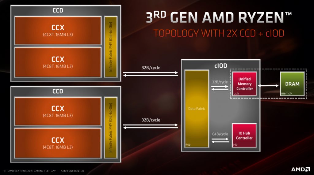
Below is a representation of the logical layout of the single CCD CPU. Each CCD contains two 4core/8thread CCX. The CCD connects to the 12nm I/O die using infinity fabric. The I/O die is responsible for handling items such as PCIe storage, USB, and contains the Unified memory controller.
The dual CCD CPUs look similar to the above except there are two CCDs each containing 4 core/8 thread CCXs.
All of the improvements to the new CPUs result in what AMD claims are about a 15% uplift in IPC performance. Typically AMD has lagged behind Intel in IPC performance.
While there are many Ryzen 3rd Gen CPUs planned, we will be testing the Ryzen 7 3700x and the Ryzen 9 3900X CPUs.
