HyperX Fury 2666MHz CL15 HX426C15FBK2 2x8GB DDR4 Review: Fast and Furious
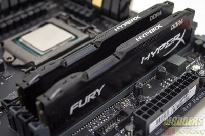
Outfitted in black aluminum heatspreaders, the HyperX Fury DDR4 is available in dual-channel and quad-channel kits for Z170 and X99 motherboards. Capacities range from 4GB to 64GB in kits of one through eight. The 1.2V HyperX Fury speed range starts at the 2133MHz (CL14) JEDEC base with faster 2400MHz and 2666MHz XMP modules (CL15) available.
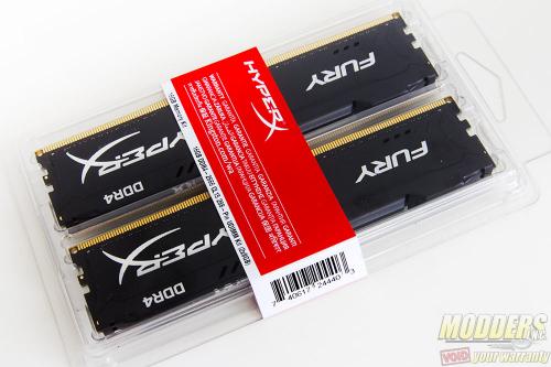
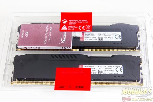
[sc:sponsor sponsor=”HyperX” product_link=”http://www.kingston.com/dataSheets/HX426C15FBK2_16.pdf” product_name=”FURY 2666MHz DDR4 Non-ECC CL15 DIMM 16 DDR4 2400 MT/s (PC4-19200) HX426C15FBK2/16″ product_price_link=”http://amzn.to/1K3wtJ8″ product_price=”$132″ ]The HyperX Fury packaging is in a completely see through blister-pack unlike previous Kingston HyperX DDR3 modules which had a black backing. Security sticker steal wraps the side edges and from the back view, the warranty and installation guide fold-out sheet is visible.
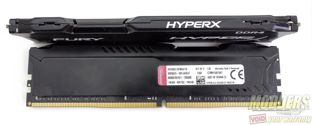
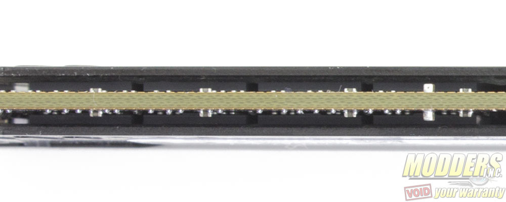
DDR4 runs cooler with lower 1.2V default voltage compared to DDR3 so it is nice to see more reasonably sized heatsinks. The total height of the HyperX Fury module is only 34.04mm and is 7.08mm thick with a standard length of 133.35mm. As as also standard of DDR4, the connector pins closer to the edge slope up compared to the middle part which are longer. This is so that uneven pressure is minimized during installation. The HyperX logo on the side is embossed while the other texts are printed white on the black heatsink. As shown on the label, this is a 2666MHz dual-channel kit.
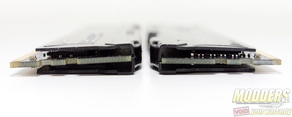
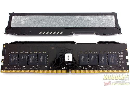
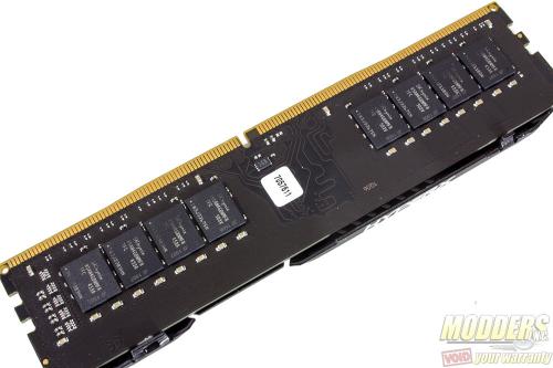
The view from the bottom reveals that the HyperX Fury is a dual-sided module and removing the heatspreader reveals a SK Hynix H5AN4G8NMFR 78-ball FBGA chips in 512 x 8 configuration per side on a black PCB measuring 133.35 x 31.25mm. There are no screws securing the heatspreader to each other and only attaches to the module via thermal adhesive tape on the side. The two piece heatspreader also slide on to each other on the top although the adhesive is the primary bond that keeps it together so you would need to replace this when modding it.
The EEPROM containing the SPD and XMP data is located at the center and here are some of the relevant information inside (via Thaiphoon Burner):
| Module Manufacturer: | Kingston |
| Module Part Number: | KHX2666C15D4/8G |
| SDRAM Manufacturer: | Hynix |
| SDRAM Components: | H5AN4G8NMFR-TFC |
| Module Manufacturing Date: | Week 32, 2015 |
| Module Manufacturing Location: | Keelung, Taiwan |
| Module Serial Number: | A0081A64h |
| Lot Number: | 0000007057611 |
| Module PCB Revision: | 00h |
| SDRAM Stepping: | Undefined |
| Fundamental Memory Class: | DDR4 SDRAM |
| Module Speed Grade: | DDR4-2666 |
| Base Module Type: | UDIMM (133.35 mm) |
| Module Capacity: | 8192 MB |
| Reference Raw Card: | B1 |
| Initial Raw Card Designer: | Micron Technology |
| Module Nominal Height: | 31 < H <= 32 mm |
| Module Thickness Maximum, Front: | 1 < T <= 2 mm |
| Module Thickness Maximum, Back: | T <= 1 mm |
| Number of DIMM Ranks: | 2 |
| Address Mapping from Edge Connector to DRAM: | Mirrored |
| SDRAM Device Package: | Standard Monolithic |
| SDRAM Device Package Type: | 78-ball FBGA |
| SDRAM Device Die Count: | Single die |
| Signal Loading: | Not specified |
| Number of Column Addresses: | 10 bits |
| Number of Row Addresses: | 15 bits |
| Number of Bank Addresses: | 2 bits (4 banks) |
| Bank Group Addressing: | 2 bits (4 groups) |
| SDRAM Device Width: | 8 bits |
| Programmed SDRAM Capacity: | 4 Gb |
| Calculated SDRAM Capacity: | 4 Gb |
| SDRAM Page Size: | 1 KB |
| Primary Memory Bus Width: | 64 bits |
| Memory Bus Width Extension: | 0 bits |
| SDRAM VDD 1.20 V operable/endurant: | Yes/Yes |
| Fine Timebase: | 0.001 ns |
| Medium Timebase: | 0.125 ns |
| CAS Latencies Supported: | 9T, 11T, 12T, 13T, 14T, 15T, 16T, 17T, 18T |
| SDRAM Minimum Cycle Time: | 0.750 ns |
| SDRAM Maximum Cycle Time: | 1.500 ns |
| Nominal SDRAM Clock Frequency: | 1333.33 MHz |
| Minimum SDRAM Clock Frequency: | 666.67 MHz |
| CAS# Latency Time (tAA min): | 11.250 ns |
| RAS# to CAS# Delay Time (tRCD min): | 12.750 ns |
| Row Precharge Delay Time (tRP min): | 12.750 ns |
| Active to Precharge Delay Time (tRAS min): | 26.250 ns |
| Act to Act/Refresh Delay Time (tRC min): | 45.000 ns |
| Normal Refresh Recovery Delay Time (tRFC1 min): | 260.000 ns |
| 2x mode Refresh Recovery Delay Time (tRFC2 min): | 160.000 ns |
| 4x mode Refresh Recovery Delay Time (tRFC4 min): | 110.000 ns |
| Short Row Active to Row Active Delay (tRRD_S min): | 5.250 ns |
| Long Row Active to Row Active Delay (tRRD_L min): | 5.250 ns |
| Long CAS to CAS Delay Time (tCCD_L min): | 5.250 ns |
| Four Active Windows Delay (tFAW min): | 22.500 ns |
| Maximum Active Window (tMAW): | 8192*tREFI |
| Maximum Activate Count (MAC): | Unlimited MAC |
| SDRAM Post Package Repair: | Not supported |
| Soft Post Package Repair: | Not supported |
| Module Thermal Sensor: | Not Incorporated |
| Manufacturer: | Microchip |
| Model: | MCP98244 |
| Revision: | 01h |
| Temperature Monitor Status: | Active |
| Current Ambient Temperature: | 28.250°C |
| Sensor Resolution: | 0.2500°C |
| Accuracy at 75°C to 95°C: | ±1°C |
| Accuracy at 40°C to 125°C: | ±2°C |
| Open-drain Event Output: | Disabled |
| 10V of VHV on A0 pin: | Supported |
| Negative Temperature Measurements: | Supported |
| Interrupt capabilities: | Supported |
| SMBus timeout period for TS access: | 25 to 35 ms |
| SPD Revision: | 1.0 |
| SPD Bytes Total: | 512 |
| SPD Bytes Used: | 384 |
| SPD Checksum (Bytes 00h-7Dh): | 038Dh (OK) |
| SPD Checksum (Bytes 80h-FDh): | 356Fh (OK) |
| JEDEC DIMM Label: | 8GB 2Rx8 PC4-2666-UB1-10 |
| FREQUENCY | CAS | RCD | RP | RAS | RC | RRDS | RRDL | CCDL | FAW |
|---|---|---|---|---|---|---|---|---|---|
| 1333 MHz | 18 | 17 | 17 | 35 | 60 | 7 | 7 | 7 | 30 |
| 1333 MHz | 17 | 17 | 17 | 35 | 60 | 7 | 7 | 7 | 30 |
| 1333 MHz | 16 | 17 | 17 | 35 | 60 | 7 | 7 | 7 | 30 |
| 1333 MHz | 15 | 17 | 17 | 35 | 60 | 7 | 7 | 7 | 30 |
| 1200 MHz | 14 | 16 | 16 | 32 | 54 | 7 | 7 | 7 | 27 |
| 1067 MHz | 13 | 14 | 14 | 28 | 48 | 6 | 6 | 6 | 24 |
| 1067 MHz | 12 | 14 | 14 | 28 | 48 | 6 | 6 | 6 | 24 |
| 933 MHz | 11 | 12 | 12 | 25 | 42 | 5 | 5 | 5 | 21 |
| 800 MHz | 9 | 11 | 11 | 21 | 36 | 5 | 5 | 5 | 18 |
| Profiles Revision: 2.0 | ||
| Profile 1 (Certified) Enables: Yes | ||
| Profile 2 (Extreme) Enables: No | ||
| Profile 1 Channel Config: 2 DIMM/channel | ||
| XMP PARAMETER | PROFILE 1 | PROFILE 2 |
|---|---|---|
| Speed Grade: | DDR4-2666 | N/A |
| RAM Clock Frequency: | 1333 MHz | N/A |
| Module VDD Voltage Level: | 1.20 V | N/A |
| Minimum SDRAM Cycle Time (tCK): | 0.750 ns | N/A |
| CAS Latencies Supported: | 16T,15T,14T,13T, 12T,11T,10T,9T |
N/A |
| CAS Latency Time (tAA): | 15T | N/A |
| RAS# to CAS# Delay Time (tRCD): | 17T | N/A |
| Row Precharge Delay Time (tRP): | 17T | N/A |
| Active to Precharge Delay Time (tRAS): | 35T | N/A |
| Active to Active/Refresh Delay Time (tRC): | 60T | N/A |
| Four Activate Window Delay Time (tFAW): | 30T | N/A |
| Short Activate to Activate Delay Time (tRRD_S): | 7T | N/A |
| Long Activate to Activate Delay Time (tRRD_L): | 7T | N/A |
| Normal Refresh Recovery Delay Time (tRFC1): | 347T | N/A |
| 2x mode Refresh Recovery Delay Time (tRFC2): | 214T | N/A |
| 4x mode Refresh Recovery Delay Time (tRFC4): | 147T | N/A |
